Method for making super junction device

Pending Publication Date: 2021-12-02
SHANGHAI HUAHONG GRACE SEMICON MFG CORP
View PDF7 Cites 2 Cited by
  • Summary
  • Abstract
  • Description
  • Claims
  • Application Information

AI Technical Summary

Benefits of technology

[0073]In addition, in the disclosure, since the gate structure is formed before the forming process of the super junction, the forming process of the source region, including the implantation and annealing driving process, can also be arranged before the forming process of the super junction. Therefore, the disclosure can further reduce the adverse influence of the thermal process of the source region driving process on the super junction, and thus can further improve the performance of the device.
[0074]By arranging the process sequence of the gate structure, the disclosure can not only obtain the beneficial effect related to the reduction of the thermal process of the super junction, but also can save the mask, which will be specifically described as follows:
[0075]Firstly, the mask for the photolithography definition process of the field oxide described above can be saved.
[0076]Secondly, when the gate structure is formed on the wafer firstly and then the body region is formed, the gate structure can b

Problems solved by technology

With the continuous reduction of the pitch of the super junction, the problem caused by counter dope formed by the mutual diffusion of P-type and N-type dope of P-type and N-type pillars in the thermal processes becomes more and more serious, which

Method used


Image

  • Method for making super junction device
  • Method for making super junction device
  • Method for making super junction device

Examples


Example

[0101]Embodiment 1 of the disclosure provides a method for making a super junction device.

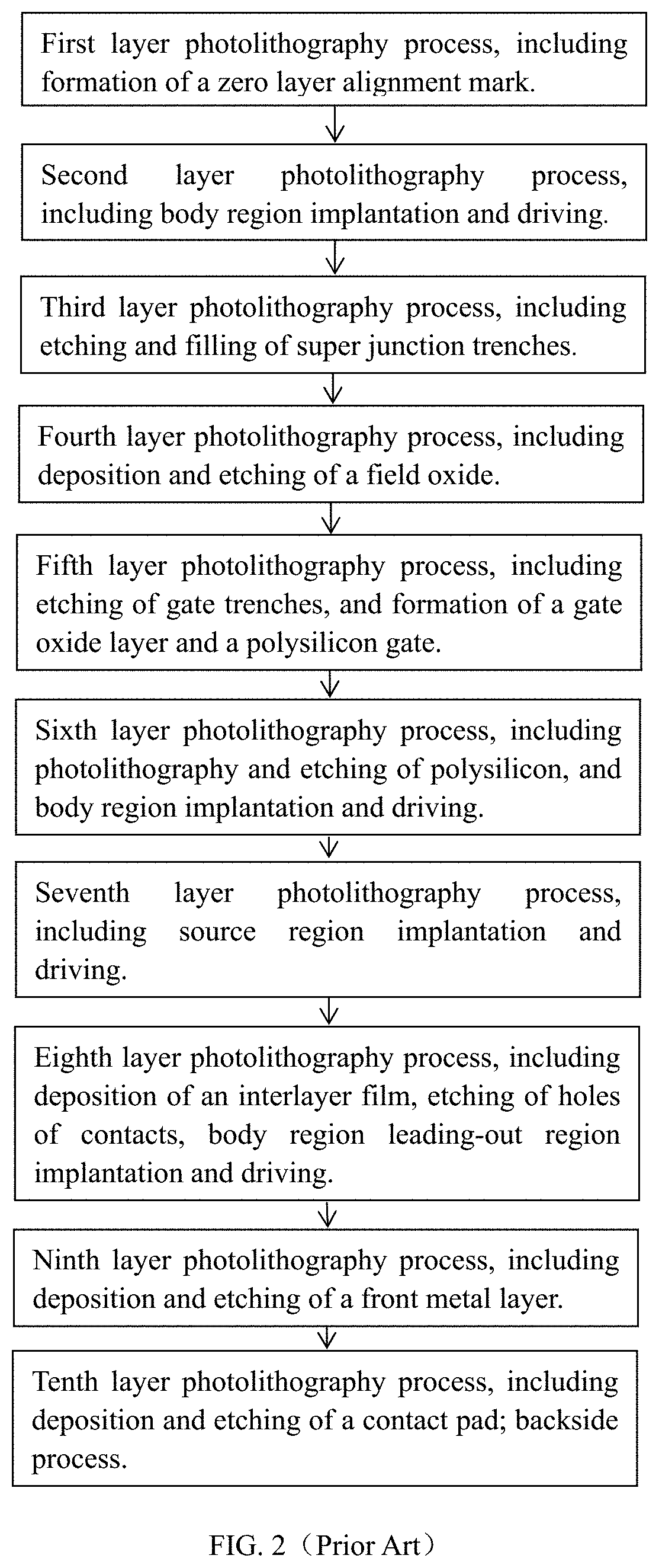
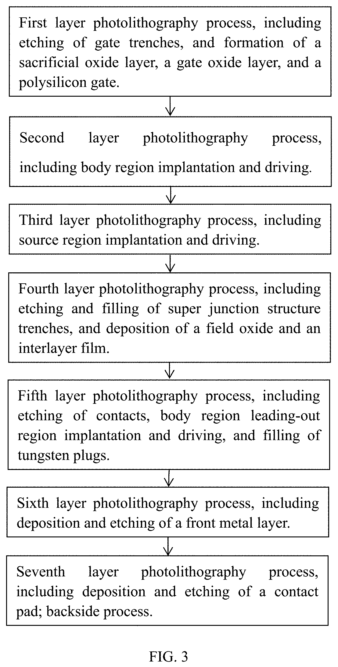
[0102]Referring to FIG. 3, it is a flowchart of the method for making the super junction device according to embodiment 1 of the disclosure. Steps are illustrated in FIG. 3 according to photolithography process levels. One photolithography process level includes a plurality of specific process steps. The photolithography process corresponding to only one mask is performed at one photolithography process level. Referring to FIG. 4A to FIG. 4N, they are schematic structural views of a device in each step of the method for making the super junction device according to embodiment 1 of the disclosure. The method for making the super junction device according to embodiment 1 of the disclosure includes the following steps:

[0103]In step 1, the gate structure is formed. The gate structure is a trench gate. The forming process of the trench gate includes the following steps:

[0104]A first conducting type ...

Example

[0166]Embodiment 2 of the disclosure provides a method for making a super junction device.

[0167]Referring to FIG. 5, it is a flowchart of the method for making the super junction device according to embodiment 2 of the disclosure. For the schematic structural view of the device in each step in the method for making the super junction device according to embodiment 2 of the disclosure, please also refer to FIG. 4A to FIG. 4N. The method for making the super junction device according to embodiment 2 of the disclosure includes the following steps:

[0168]Referring to FIG. 4A, a first conducting type first epitaxial layer 2 is provided.

[0169]The first epitaxial layer 2 is formed on a semiconductor substrate 1. Generally, the semiconductor substrate 1 is a silicon substrate.

[0170]A photolithography process is performed by adopting a zero layer mask and a zero layer alignment mark is formed. The process of forming the zero layer alignment mark corresponds to the first layer photolithography...

Example

[0222]Embodiment 3 of the disclosure provides a method for making a super junction device.

[0223]Referring to FIG. 6, it is a flowchart of the method for making the super junction device according to embodiment 3 of the disclosure. For the schematic structural view of the device in each step in the method for making the super junction device according to embodiment 3 of the disclosure, please also refer to FIG. 4A to FIG. 4N. The method for making the super junction device according to embodiment 3 of the disclosure includes the following steps:

[0224]In step 1, the gate structure is formed. The gate structure is a trench gate. The forming process of the trench gate includes the following steps:

[0225]A first conducting type first epitaxial layer 2 is provided and a photolithography process is performed to define the forming area of gate trenches 201.

[0226]Referring to FIG. 4A, a first conducting type first epitaxial layer 2 is provided. The first epitaxial layer 2 is formed on the sur...


PUM


Abstract

A method for making a super junction device includes the following steps: step 1: forming a trench gate, in the forming process of the trench gate, a polysilicon gate being used to fill gate trenches and then first flattening being performed and the width of the gate trench at the leading-out position of the gate structure satisfies the requirement of forming contacts; and step 2: forming a super junction, in the forming process of the super junction, a second epitaxial layer being used to fill a super junction trench and then second flattening being performed. The method can realize an all flat process, can conveniently arrange the trench gate process before the forming process of the super junction, can decrease the thermal processes after the formation of the super junction, can save the mask and can decrease the process cost.

Description

CROSS-REFERENCE TO RELATED APPLICATION[0001]This application claims the priority to Chinese patent application No. CN 202010475492.5 filed at CNIPA on May 29, 2020, and entitled “METHOD FOR MAKING SUPER JUNCTION DEVICE”, the disclosure of which is incorporated herein by reference in entirety.TECHNICAL FIELD[0002]The disclosure relates to a method for making a semiconductor integrated circuit, in particular to a method for making a super junction device.BACKGROUND[0003]A super junction consists of alternately arranged P-type thin layers (also known as P-type pillars) and N-type thin layers (also known as N-type pillars) formed in a semiconductor substrate. Devices using a super junction are super junction devices, for example, super junction MOSFETs. By adopting the reduced surface field (Resurf) technique with balanced P-type and N-type thin layer charges, the reverse breakdown voltage of the device can be improved and the on resistance can be at the same time maintained to be small...

Claims


Application Information

Patent Timeline
IPC IPC(8): H01L29/06H01L29/40H01L29/423
CPCH01L29/0607H01L29/4236H01L29/401H01L29/66734H01L29/7813H01L29/0634H01L29/7811H01L29/1095
Inventor LI, HAO
Owner SHANGHAI HUAHONG GRACE SEMICON MFG CORP
Why Eureka
Try Eureka