Power conversion device

Active Publication Date: 2021-12-02
MITSUBISHI ELECTRIC CORP
View PDF0 Cites 0 Cited by
  • Summary
  • Abstract
  • Description
  • Claims
  • Application Information

AI Technical Summary

Benefits of technology

The power conversion device described in this patent can reduce the noise generated during power conversion and make the device smaller.

Problems solved by technology

The higher-frequency driving of a power conversion device has advantages that enable high-speed control such as real-time control, but also has disadvantages including the increase in heat generated in semiconductor switching elements due to the increase in switching loss, and the increase in heat generated in electrical components such as a reactor and a transformer due to the increase in copper loss and iron loss.

Method used


Image

  • Power conversion device
  • Power conversion device

Examples


embodiment 1

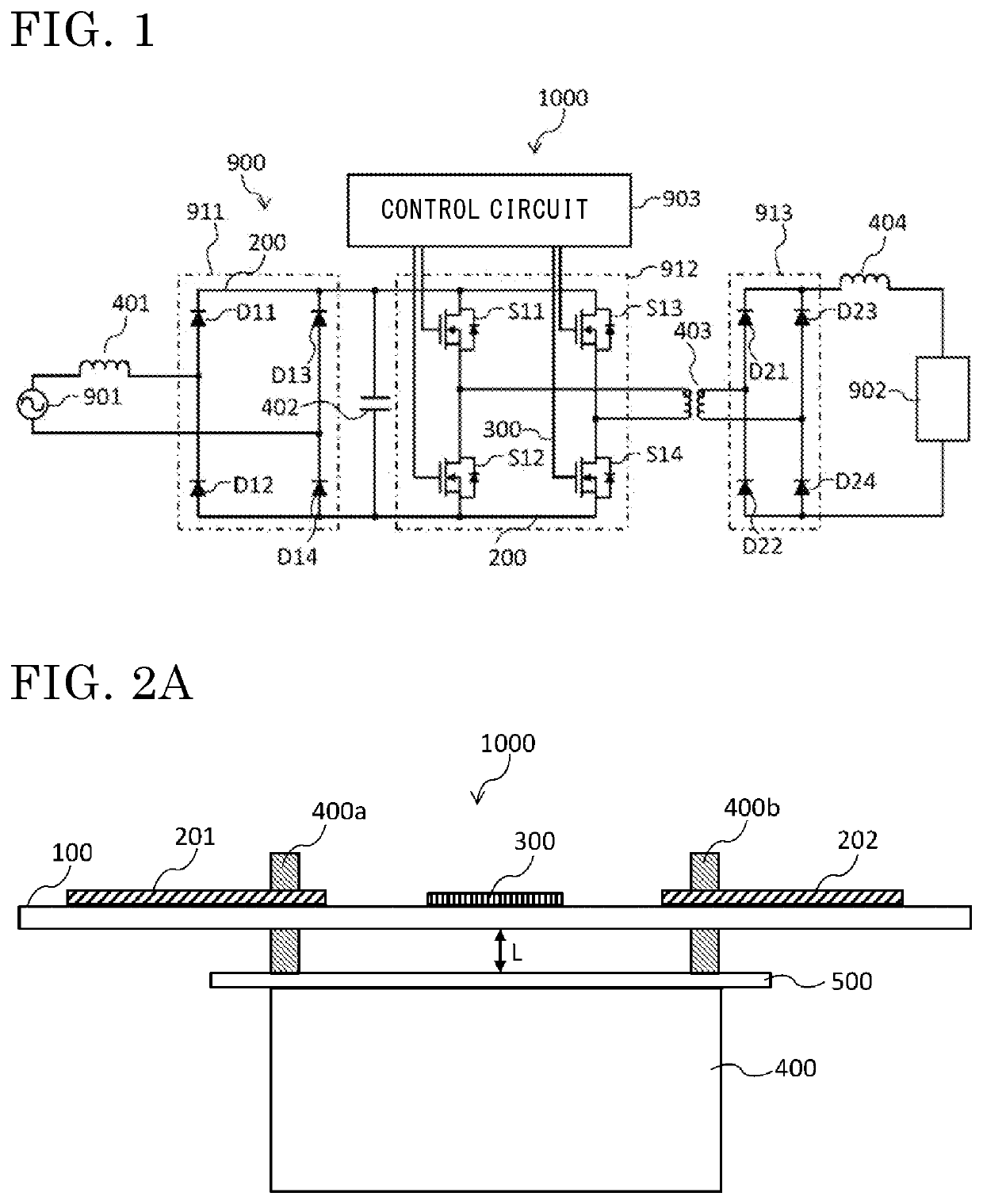
[0013]Hereinafter, embodiment 1 will be described on the basis of FIGS. 1 to 2B. FIG. 1 is a schematic circuit diagram showing a power conversion device according to embodiment 1. A power conversion device 1000 converts AC power outputted from an AC power supply 901 to DC power having a desired voltage and supplies the resultant DC power to a load 902, and includes a main circuit 900 in which current from the AC power supply 901 flows, and a control circuit 903 which controls driving of a plurality of switching elements S11 to S14 provided in the main circuit 900. The plurality of switching elements S11 to S14 and various main circuit components are connected to one another through main circuit wires 200 so as to form the main circuit 900. Additionally, the plurality of switching elements S11 to S14 and the control circuit 903 are connected via respective control wires 300 which are electrically insulated from the main circuit wires 200. Note that the “main circuit components” in em...

embodiment 2

[0035]Hereinafter, embodiment 2 will be discussed on the basis of FIG. 3. The components identical to or corresponding to those in FIGS. 1 to 2B are denoted by the same reference characters and the description thereof is omitted. FIG. 3 is a partial side view showing a power conversion device according to embodiment 2. FIG. 3 shows the periphery of an arbitrary main circuit component 400 of a power conversion device 1010 corresponding to the power conversion device 1000 in embodiment 1, as viewed from the side thereof. In embodiment 2, terminals for connecting the main circuit component, and the first main circuit wire and the second main circuit wire, are each divided into two divided terminals.

[0036]The main circuit component 400 is provided with a first divided terminal 400a1 and a first divided terminal 400b1 at one end and another end in the plane direction of the substrate 100. The first divided terminal 400a1 and the first divided terminal 400b1 extend toward the substrate 10...


PUM


Abstract

An object is to obtain a power conversion device that can suppress the generation of noise due to coupling and achieve the size reduction of a substrate. In a power conversion device, a main circuit wire for connecting main circuit components to form a main circuit includes a first main circuit wire and a second main circuit wire wired so as to be separated from each other on a substrate. A control wire is wired between the first main circuit wire and the second main circuit wire so as to be insulated therefrom, and the first main circuit wire and the second main circuit wire are connected to each other via the main circuit component placed so as to be separated from the control wire in the thickness direction of the substrate.

Description

TECHNICAL FIELD[0001]The present disclosure relates to a power conversion device.BACKGROUND ART[0002]In recent years, the higher-frequency driving of a power conversion device has been promoted, and wide-gap semiconductors such as Silicon Carbide (SiC) and Gallium Nitride (GaN) are used as switching elements of inverter circuits. The higher-frequency driving of a power conversion device has advantages that enable high-speed control such as real-time control, but also has disadvantages including the increase in heat generated in semiconductor switching elements due to the increase in switching loss, and the increase in heat generated in electrical components such as a reactor and a transformer due to the increase in copper loss and iron loss.[0003]In response to this, a power conversion device is proposed, the power conversion device including a recess for housing an electrical component therein, a cover having a semiconductor switching element to be mounted on a flat surface on the ...

Claims


Application Information

Patent Timeline
IPC IPC(8): H02M7/00H02M3/28
CPCH02M7/003H02M3/28H02M1/007H02M3/33573H02M3/003H02M7/06H02M1/0048H02M5/458H02M1/4258H05K1/0216H05K1/144H05K1/0219H05K2201/09972H05K2201/09336H05K2201/042H05K2201/2036H05K2201/0394H05K2201/10378Y02B70/10
InventorHAYASHI, RYOMA
OwnerMITSUBISHI ELECTRIC CORP