Display panel, manufacturing method thereof, and display device

a technology of display panel and manufacturing method, applied in the field of display technology, to achieve the effect of optimizing the area design, improving the integration of the display panel, and maximizing the area of functional components

Pending Publication Date: 2021-12-23
WUHAN CHINA STAR OPTOELECTRONICS TECH CO LTD
View PDF1 Cites 0 Cited by
  • Summary
  • Abstract
  • Description
  • Claims
  • Application Information

AI Technical Summary

Benefits of technology

[0026]In the display panel, the manufacturing method thereof, and the display device provided by the present disclosure, beneficial effect of the present disclosure is that the functional component groups are integrated into the subpixel units, improving integration of the display panel. Furthermore, the shapes of part of the functional components are made into shapes of the alignment marks, realizing multiplexing of mass transfer alignment marks, and other functional components not multiplexed as the marks are kept in a maximized area design. Therefore, there is no need to occupy additional pixel space for independently manufacturing the mass transfer alignment marks, which can ensure areas of the functional components to be maximized. Moreover, design degree of freedom of each display subpixel units can be increased, which is conducive to increasing space of the subpixel units, thereby realizing high PPI display.

Problems solved by technology

However, configuration of the alignment marks can additionally occupy space of display pixels.

Method used


Image

  • Display panel, manufacturing method thereof, and display device
  • Display panel, manufacturing method thereof, and display device
  • Display panel, manufacturing method thereof, and display device

Examples


Embodiment Construction

[0038]The descriptions of embodiments below refer to accompanying drawings in order to illustrate certain embodiments which the present disclosure can implement. The directional terms of which the present disclosure mentions, for example, “top”, “bottom”, “upper” , “lower”, “front”, “rear”, “left”, “right”, “inside”, “outside”, “side”, etc., only refer to directions of the accompanying figures. Therefore, the used directional terms are for illustrating and understanding the present disclosure, but not for limiting the present disclosure. In the figures, units with similar structures are indicated by the same reference numerals.

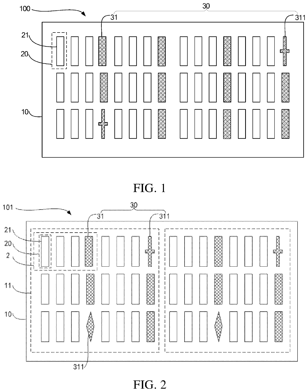
[0039]In one embodiment, a display panel 100 is provided. As illustrated in FIG. 1, the display panel 100 includes a driving backplate 10, a plurality of subpixel units 20, and functional component groups 30. The plurality of subpixel units 20 are disposed on the driving backplate 10, and the functional component groups 30 are disposed between the adjacent sub...


PUM


Abstract

A display panel, a manufacturing method thereof, and a display device are provided. The display panel includes a driving backplate, functional component groups, and micro-LED chips. The functional component groups are integrated in regions where the micro-LED chips are not disposed and are multiplexed as alignment marks. In a mass transfer process of the micro-LED chips, the alignment marks are prevented from additionally occupying pixel space by using part of functional components multiplexed as the alignment marks under a precondition of ensuring alignment accuracy.

Description

FIELD OF INVENTION[0001]The present disclosure relates to the field of display technology, and particularly relates to a display panel, a manufacturing method thereof, and a display device.BACKGROUND OF INVENTION[0002]With development of micro light emitting diode (micro-LED) technology, dimensions of micro-LED chips are manufactured increasingly smaller, pixels per inch (PPI) of corresponding micro-LED display devices able to be manufactured thereof are increasingly higher, pitches between the micro-LED chips on driving backplates are increasingly smaller, and a number of the micro-LED chips is increasingly greater. In current mass transfer technology, a transfer area is about one inch, and completely manufacturing one screen usually needs a plurality of repeated transfer processes. Furthermore, in the transfer processes, alignment marks need to be designed on the driving backplates in advance to ensure transfer accuracy. However, configuration of the alignment marks can additional...

Claims


Application Information

Patent Timeline
Patent Type & Authority Applications(United States)
IPC IPC(8): H01L25/16G06K9/00
CPCH01L25/167H01L33/52G06K9/0004H01L25/0753G06V40/1318H01L2933/005G06V40/1306G06V40/1359G06V40/1365
Inventor ZHONG, LIZHA, GUOWEI
Owner WUHAN CHINA STAR OPTOELECTRONICS TECH CO LTD
Why Eureka
Try Eureka