Flexible display panel and manufacturing method thereof

a display panel and flexible technology, applied in the field of display technologies, can solve problems affecting the life of the display panel, achieve the effects of reducing the stress concentration effect of the inorganic film layer, reducing the slope of the sidewall of the dam, and effectively relieving the stress

Active Publication Date: 2021-12-30
WUHAN CHINA STAR OPTOELECTRONICS SEMICON DISPLAY TECH CO LTD
View PDF0 Cites 1 Cited by
  • Summary
  • Abstract
  • Description
  • Claims
  • Application Information

AI Technical Summary

Benefits of technology

[0018]An embodiment of the present application fills the protective film in a stress concentration area of the inorganic film layer at the corner of the dam. On one hand, it can effectively slow down the slope of the sidewall of the dam and reduce stress concentration effect of the inorganic film layer in the upper packaging structure to a certain extent. On the other hand, when the protective film is subjected to stress, it can effectively relieve the stress and weaken or even eliminate stress effect of the packaging structure on the anode layer at the corner of the dam. By slowing down stress concentration at the corner of the dam from the above two aspects, issues of easy peeling of the anode layer at the dam can be effectively improved, and packaging yield of the flexible display panel can be improved.

Problems solved by technology

Since a light emitting material of the OLED device is very sensitive to water and oxygen, a small amount of water and oxygen invasion will cause rapid attenuation and aging of the device, thereby affecting its life.

Method used


Image

  • Flexible display panel and manufacturing method thereof
  • Flexible display panel and manufacturing method thereof
  • Flexible display panel and manufacturing method thereof

Examples


first embodiment

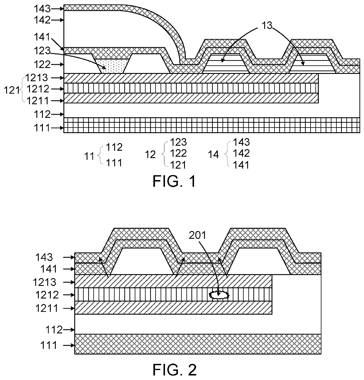
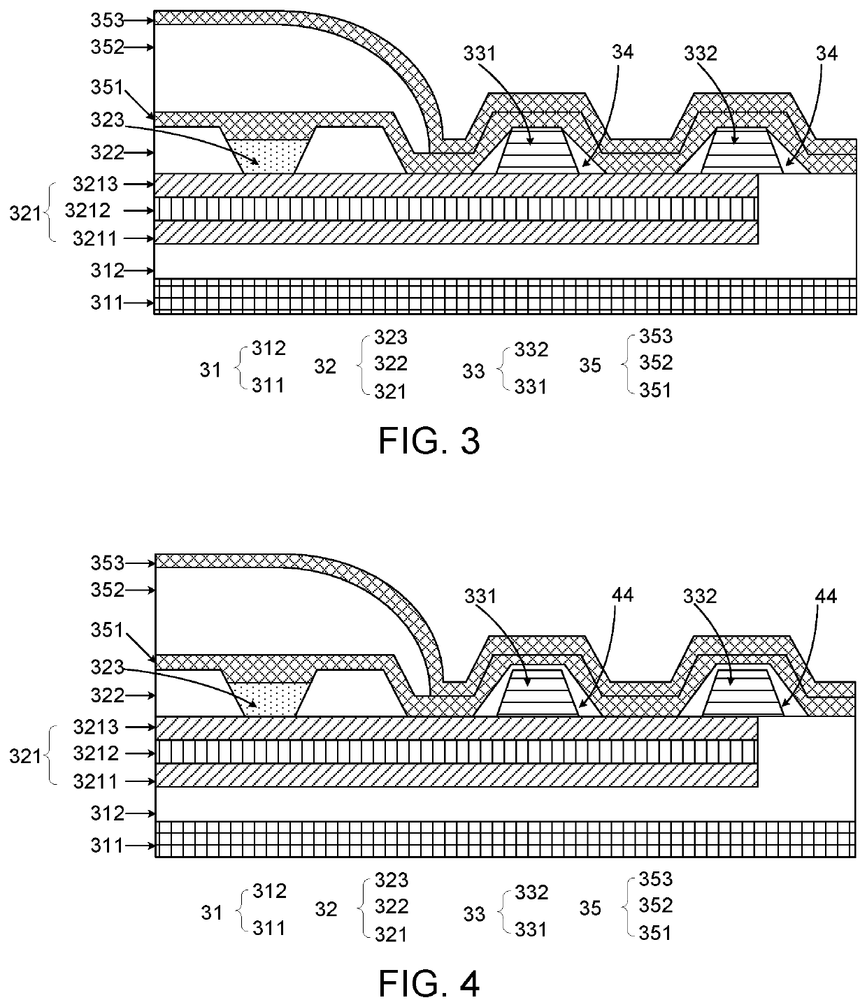
[0030]Referring to FIG. 3, which is a cross-sectional view of a part of a layered structure of a flexible display panel of the present application. The flexible display panel includes an array substrate 31, a light emitting device layer 32, a dam group 33, a protective film 34, and a packaging structure 35.

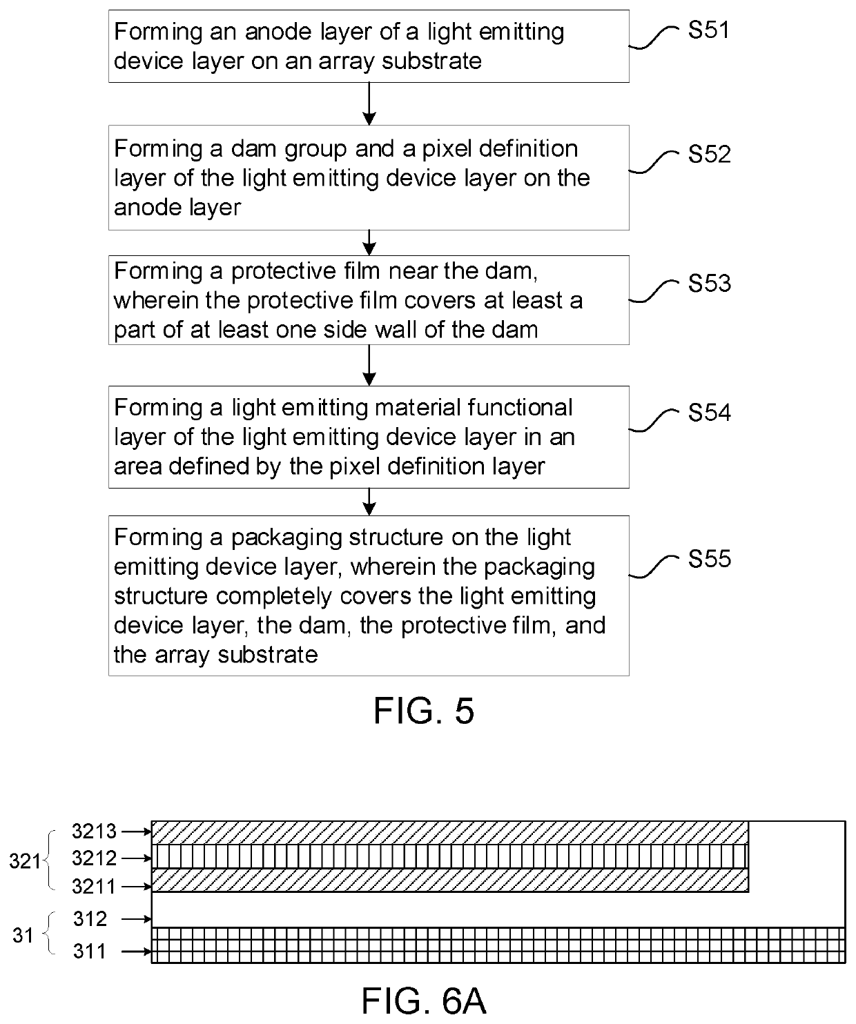
[0031]In an embodiment, the array substrate 31 is a thin film transistor (TFT) array substrate and includes a TFT array layer 311 and a planarization layer (PLN) 312 formed on the TFT array layer 311. The TFT array layer 311 is a driving circuit of the flexible display panel and is an important component of the display panel. The planarization layer 312 mainly plays a role of flattening in-plane segment difference caused by patterns of various layers on the TFT array substrate 31, isolating TFTs from the light emitting device layer 32, and preventing electric field interference. For a manufacturing process of the array substrate 31, reference may be made to an existing process, wh...

second embodiment

[0045]Referring to FIG. 4, a cross-sectional view of a part of a layered structure of a flexible display panel according to the present application is provided. The difference from the embodiment shown in FIG. 3 is that, in this embodiment, a protective film 44 completely covers the dam group 33. Specifically, the protective film 44 covers both side walls and a top surface of the first dam 331 and covers both side walls and a top surface of the second dam 332. A thickness of the protective film 44 covering the top surface of the corresponding dam is designed to be about 1 μm. That is, all exposed surfaces of the corresponding dam are covered with a protective film. This design can not only relieve stress concentration at the corner of the corresponding dam, but also relieve the stress at the top surface of the corner of the dam. This is more conducive to slowing down the stress effect of the inorganic film layer in the packaging structure, and effectively improving the issue of the ...


PUM

PropertyMeasurementUnit
thicknessaaaaaaaaaa
electric fieldaaaaaaaaaa
thicknessaaaaaaaaaa

Abstract

A flexible display panel and a manufacturing method thereof are provided. By filling a protective film in a stress concentration area of an inorganic film layer at a corner of a dam, a slope of a side wall of the dam can be effectively reduced, and stress concentration effect of the inorganic film layer in an upper packaging structure is reduced to a certain extent. When the protective film is subjected to stress, it can effectively relieve the stress and weaken or even eliminate stress effect of the packaging structure on an anode layer at a corner of the dam.

Description

CROSS-REFERENCE TO RELATED APPLICATION[0001]This application claims the priority of Chinese Application No. 201910747074.4 filed on Aug. 14, 2019 and titled “FLEXIBLE DISPLAY PANEL AND MANUFACTURING METHOD THEREOF”, which is incorporated herein by reference in its entirety.FIELD OF INVENTION[0002]The present disclosure relates to the field of display technologies, and more particularly to a flexible display panel and a manufacturing method thereof.BACKGROUND OF INVENTION[0003]With the rapid development of organic light emitting diode (OLED) display technology, curved surface and flexible display products are rapidly entering the market, and technological updates in related fields are also changing with each passing day. OLED devices are diode devices that use organic light emitting materials to drive light through carrier injection and recombination under drive of an electric field. OLED devices have attracted widespread attention due to their advantages such as light weight, thin t...

Claims


Application Information

Patent Timeline
Patent Type & Authority Applications(United States)
IPC IPC(8): H01L51/52H01L27/32H01L51/56
CPCH01L51/5253H01L27/3246H01L2251/308H01L51/5206H01L2251/5338H01L51/56H01L21/77H10K59/88H10K59/00H10K59/124H10K59/122H10K50/818H10K50/844H10K2102/311H10K50/81H10K71/00H10K2102/103
Inventor LU, RUIYIN, XUEBING
Owner WUHAN CHINA STAR OPTOELECTRONICS SEMICON DISPLAY TECH CO LTD
Why Eureka
Try Eureka