Bidirectional switch, electrical device, and multi-level inverter

a multi-level inverter and bi-directional switch technology, applied in the direction of dc-dc conversion, solid-state devices, dc-dc conversion, etc., can solve the problem of increasing the on-state resistance at the time, and achieve the effect of reducing the current collaps

Pending Publication Date: 2021-12-30
PANASONIC INTELLECTUAL PROPERTY MANAGEMENT CO LTD
View PDF0 Cites 0 Cited by
  • Summary
  • Abstract
  • Description
  • Claims
  • Application Information

AI Technical Summary

Benefits of technology

The patent text describes a new type of switch called a bidirectional switch, which can reduce the current collapse when used in an electrical device. The invention also includes a multi-level inverter that can improve the performance of the device by reducing the current collapse.

Problems solved by technology

When used with its substrate electrically floating, for example, the bidirectional switch element of Patent Literature 1 may produce a current collapse that causes an increase in its ON-state resistance at the time of switching.

Method used


Image

  • Bidirectional switch, electrical device, and multi-level inverter
  • Bidirectional switch, electrical device, and multi-level inverter
  • Bidirectional switch, electrical device, and multi-level inverter

Examples


first embodiment

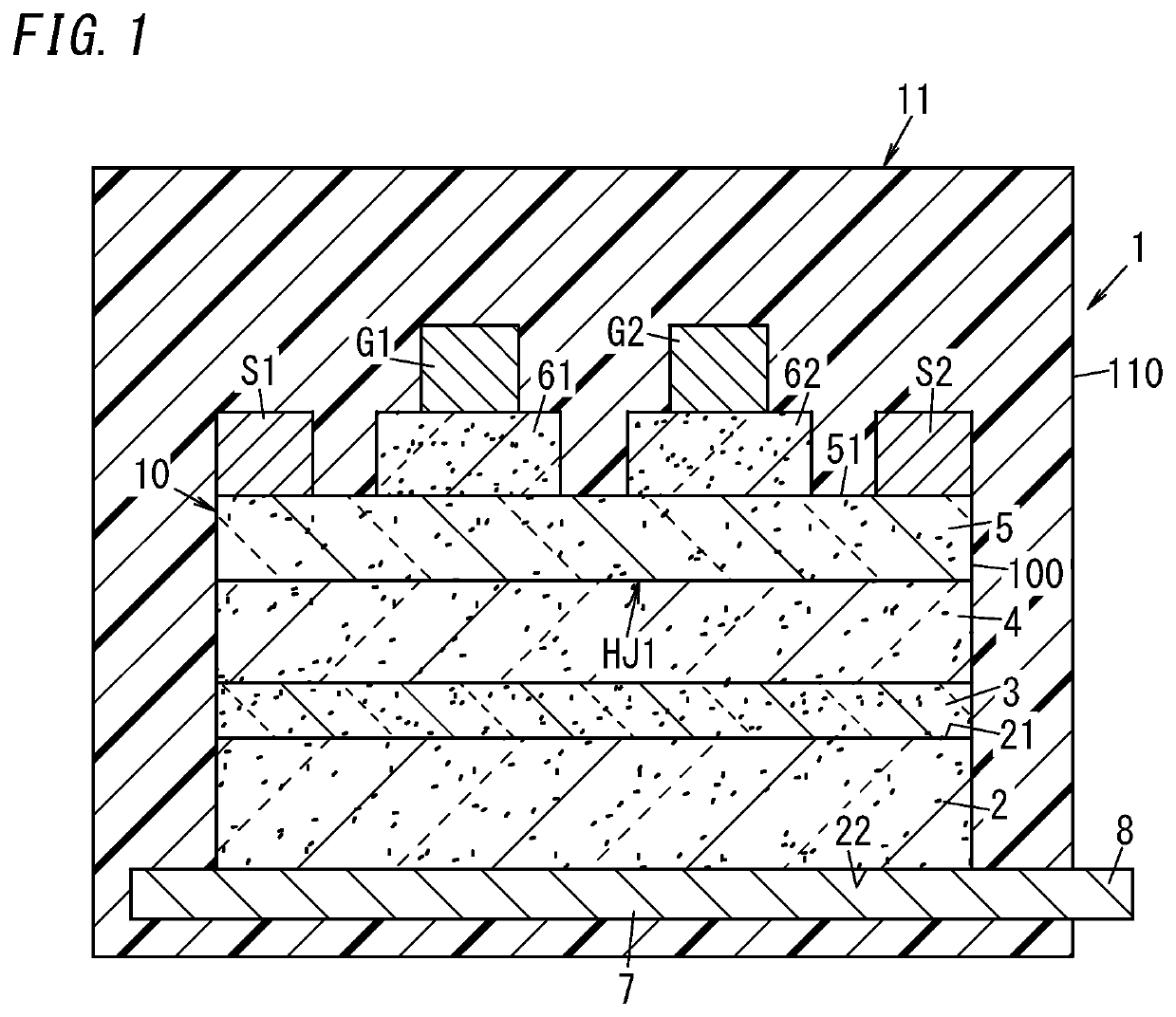
[0038]A bidirectional switch 1 according to a first embodiment will be described with reference to FIG. 1.

[0039](1.1) Overview

[0040]The bidirectional switch 1 includes a bidirectional switch element 10 and a package 11 to protect the bidirectional switch element 10. The bidirectional switch element 10 includes a substrate 2, a GaN layer 4, an AlGaN layer 5, a first source electrode S1, a first gate electrode G1, a second gate electrode G2, a second source electrode S2, a first p-type Alx1Ga1-x1N layer 61 (where 0≤x1x2Ga1-x2N layer 62 (where 0≤x21 according to the first embodiment, x1=x2. The package 11 includes a first source terminal, a first gate terminal, a second source terminal, and a second gate terminal, to which the first source electrode S1, first gate electrode G1, second source electrode S2, and second gate electrode G2 of the bidirectional switch element 10 are respectively connected. The package 11 further includes a terminal 8 connected to the substrate 2 of the bidire...

second embodiment

[0111]An electrical device 300a according to a second embodiment will be described with reference to FIGS. 7, 8, 9A, and 9B. The electrical device 300a is implemented as a switch system.

[0112](2.1) Overall Configuration for Electrical Device

[0113]The electrical device 300a includes a bidirectional switch device 101 and a control system 302 for controlling the bidirectional switch device 101.

[0114]As shown in FIG. 7, the bidirectional switch device 101 is formed by connecting a plurality of (e.g., three) bidirectional switches 1 in parallel. In this embodiment, the bidirectional switch device 101 includes a pair of main terminals 111, 112 and also includes a parallel circuit of the plurality of bidirectional switches 1 between the pair of main terminals 111, 112. The bidirectional switches 1 have the same configuration as the bidirectional switch 1 according to the first embodiment, and description thereof will be omitted herein as appropriate. In FIG. 7, the terminal 8 shown in FIG....

third embodiment

[0163]Next, an electrical device 300b according to a third embodiment will be described with reference to FIG. 14. The electrical device 300b is implemented as a switch system.

[0164]The electrical device 300b according to the third embodiment is almost the same as the electrical device 300a according to the second embodiment except that the electrical device 300b according to the third embodiment includes a control system 302a instead of the control system 302, which is a major difference from the electrical device 300a according to the second embodiment. In the following description, any constituent element of the electrical device 300b according to this third embodiment, having the same function as a counterpart of the electrical device 300a according to the second embodiment described above, will be designated by the same reference numeral as that counterpart's, and description thereof will be omitted herein. The bidirectional switch 1 has the same configuration as the bidirectio...


PUM

PropertyMeasurementUnit
off-axis angleaaaaaaaaaa
thicknessaaaaaaaaaa

Abstract

A GaN layer is formed over the substrate. An AlGaN layer is formed on the GaN layer. A first source electrode, a first gate electrode, a second gate electrode, and a second source electrode are formed on or over the AlGaN layer. A first p-type Alx1Ga1-x1N layer where 0≤x1<1 is interposed between the first gate electrode and the AlGaN layer. A second p-type Alx2Ga1-x2N layer where 0≤x2<1 is interposed between the second gate electrode and the AlGaN layer. The substrate is electrically insulated from all of the first source electrode, the second source electrode, the first gate electrode, and the second gate electrode. The bidirectional switch further includes a terminal used to connect the substrate to a fixed potential node. The terminal is connected to the substrate.

Description

CROSS-REFERENCE OF RELATED APPLICATIONS[0001]This application is the U.S. National Phase under 35 U.S.C. § 371 of International Patent Application No. PCT / JP2019 / 032985, filed on Aug. 23, 2019, which in turn claims the benefit of Japanese Application No. 2018-210724, filed on Nov. 8, 2018, Japanese Application No. 2019-016440, filed on Jan. 31, 2019 and Japanese Application No. 2019-079572, filed on Apr. 18, 2019, the entire disclosures of which Applications are incorporated by reference herein.TECHNICAL FIELD[0002]The present disclosure generally relates to a bidirectional switch, an electrical device, and a multi-level inverter, and more particularly relates to a bidirectional switch including two gate electrodes, an electrical device including the bidirectional switch, and a multi-level inverter including the bidirectional switch.BACKGROUND ART[0003]A bidirectional switch element, which is a double-gate (also called “dual-gate”) semiconductor element, has been proposed in the art...

Claims


Application Information

Patent Timeline
Patent Type & Authority Applications(United States)
IPC IPC(8): H02M7/483H02M1/08H01L29/778
CPCH02M7/483H01L29/7786H02M1/08H01L21/822H01L27/04H02M7/487H02M3/158H01L29/1066H01L29/42316H01L29/2003Y02B70/10
Inventor KINOSHITA, YUSUKEYAMADA, YASUHIROICHIRYU, TAKASHINOMURA, MASANORIISHIDA, HIDETOSHI
Owner PANASONIC INTELLECTUAL PROPERTY MANAGEMENT CO LTD
Why Eureka
Try Eureka