Operable GaN Devices

A gallium nitride and device technology, applied in the field of technology and circuits, can solve the problems of high electron mobility, invalid semiconductor devices, and unusable GaN semiconductor devices, etc.

Active Publication Date: 2018-10-19
INFINEON TECH AUSTRIA AG
View PDF5 Cites 0 Cited by
  • Summary
  • Abstract
  • Description
  • Claims
  • Application Information

AI Technical Summary

Problems solved by technology

However, semiconductor devices that rely on the combination of a GaN substrate and a common substrate suffer from exceptionally high-speed trap
High-speed traps can render GaN-based semiconductor devices ineffective and useless as high electron mobility field-effect transistors (HEMTs)
For example, current collapse in a GaN-based semiconductor device can make the R of the GaN-based semiconductor device DSON increases by a factor of 100, and practically renders GaN semiconductor devices unusable for most HEMT applications

Method used


Image

  • Operable GaN Devices
  • Operable GaN Devices
  • Operable GaN Devices

Examples


Embodiment Construction

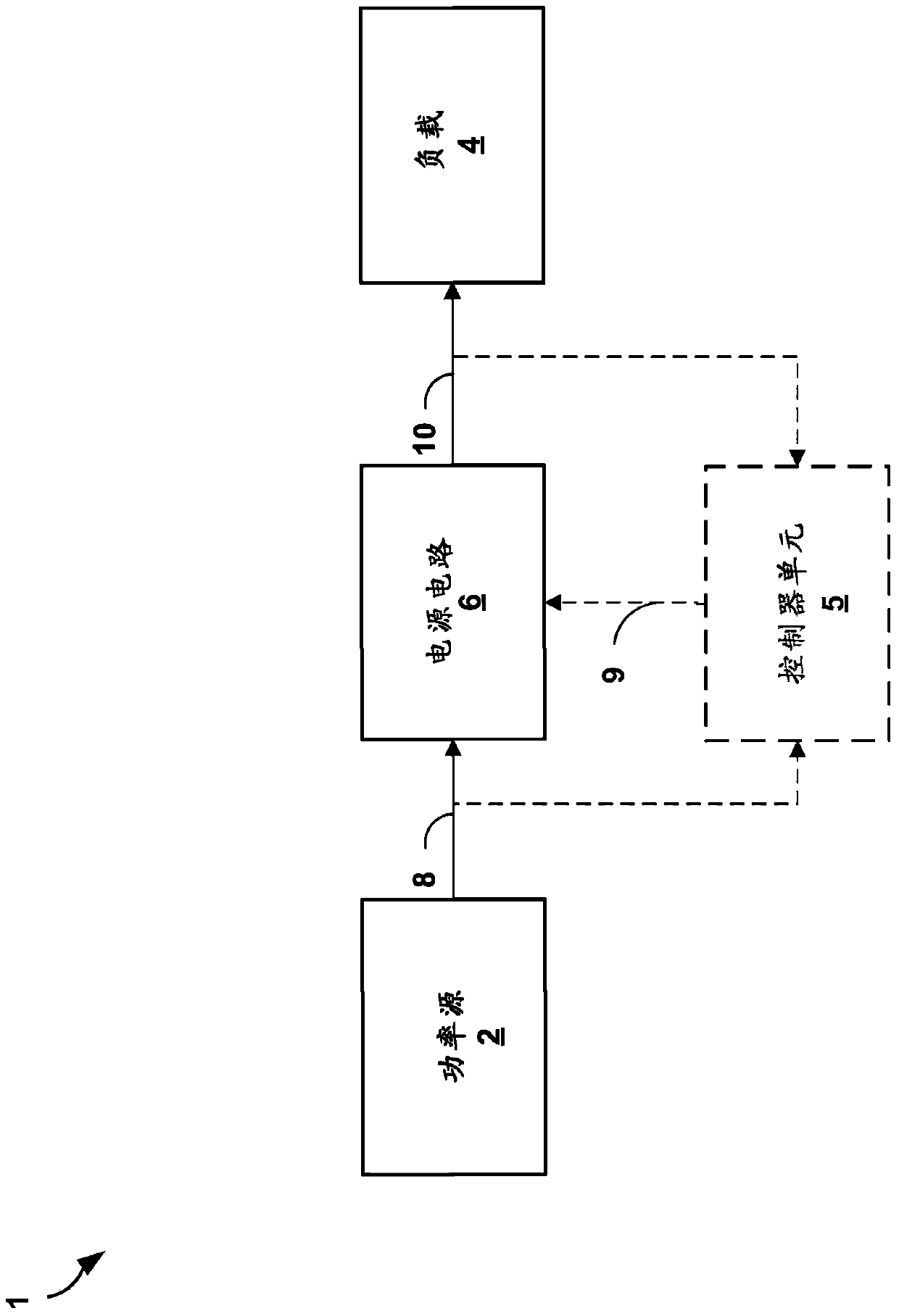
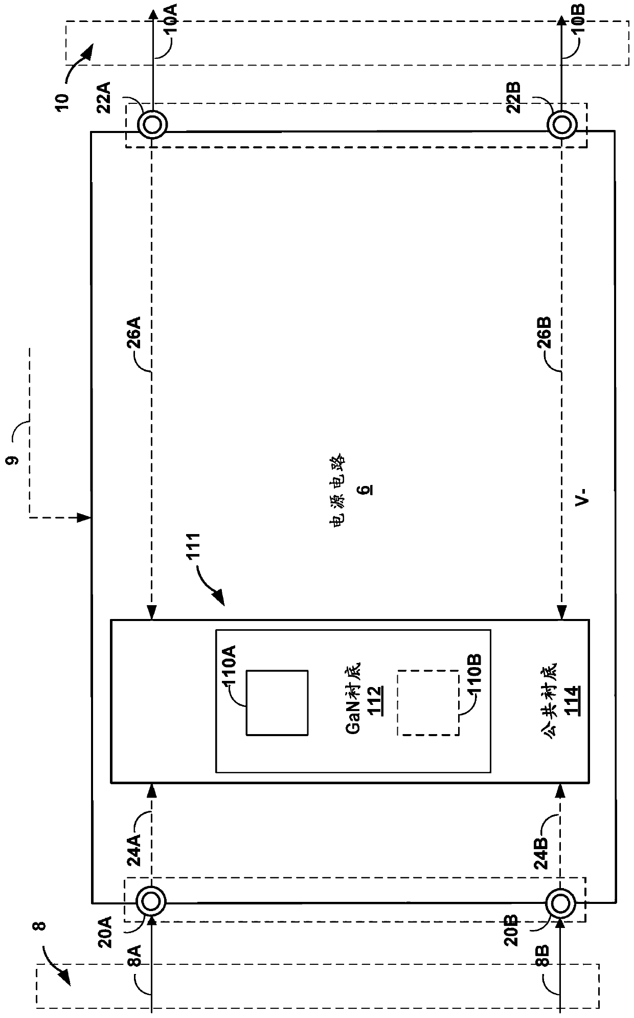
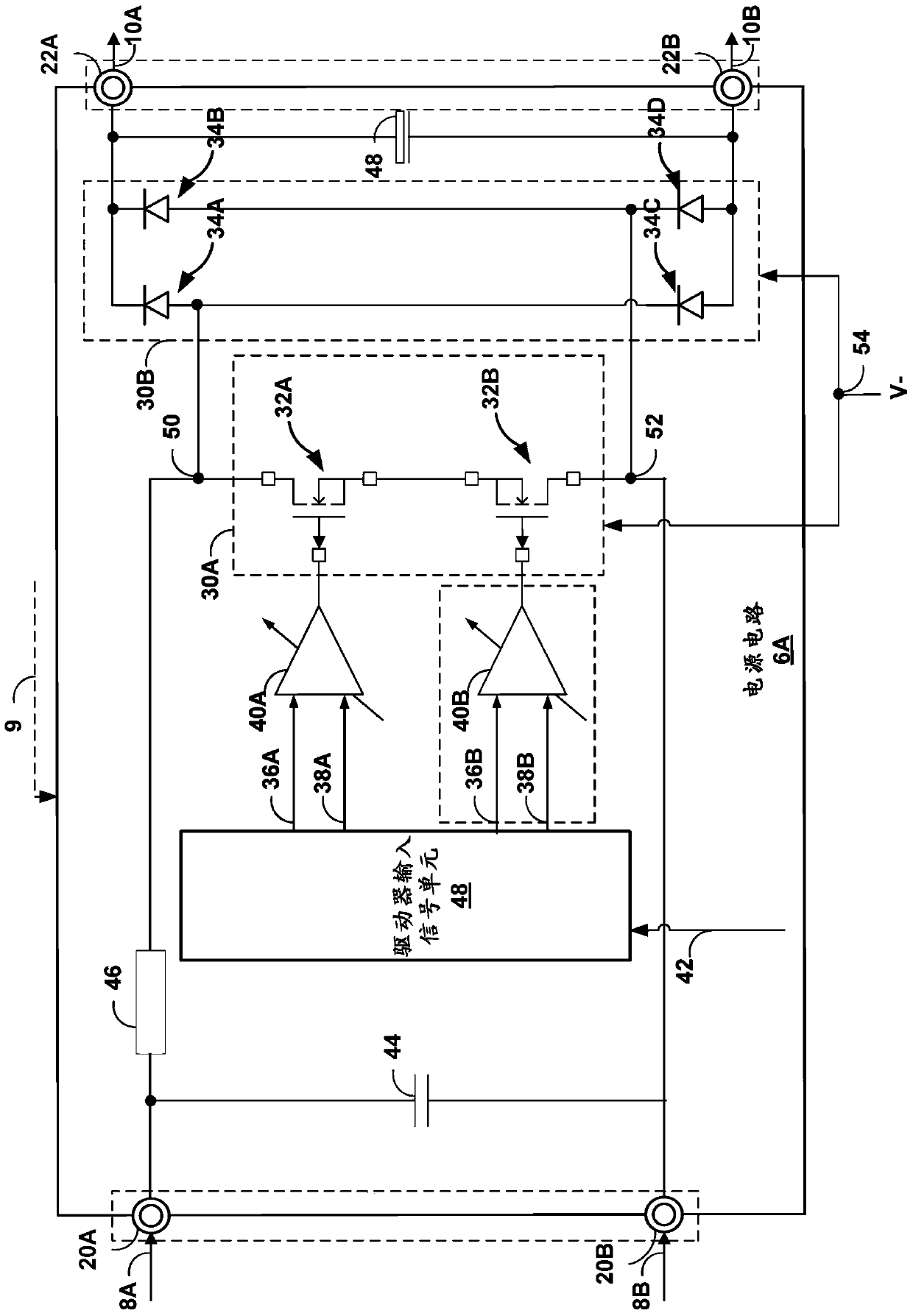
[0023] Some electronic devices (eg, transistors, diodes, switches, etc.) are semiconductor-based, or in other words, made of semiconductor materials such as silicon (Si), silicon nitride (SiC), gallium nitride (GaN), and the like. For example, a bidirectional GaN switch may include one or more GaN devices (eg, two GaN switches) having an AlGaN layer adhered to a substrate and / or a combination of substrates, such as a combination of a GaN substrate and a Si substrate. In some examples, using more than one Si substrate layer, etc., can reduce the lattice mismatch between the GaN substrate and the Si substrate.

[0024] Some advantages of using GaN-based components, such as GaN high electron mobility transistors (HEMTs), are that GaN-based components are considered high performance and low cost compared to other types of HEMTs or similar types of semiconductor components. For example, unlike other types of semiconductor components, GaN-based components can have a high saturation ...


PUM


Abstract

A power supply circuit is described that includes a semiconductor body having a common substrate and a gallium nitride (GaN) based substrate. The GaN-based substrate includes one or more GaN devices adjacent to the front side of a common substrate. The common substrate is electrically coupled to nodes of the power circuit. Nodes of the power circuit are at a specific potential that is equal to or less than a potential at one or more load terminals of the one or more GaN devices.

Description

technical field [0001] The present invention relates to techniques and circuits related to semiconductor devices. Background technique [0002] Gallium nitride (GaN) can be used as a fabrication material for semiconductor devices. A significant advantage of GaN is that GaN has strain-induced piezoelectric charges, which allow conduction channels (eg, two-dimensional electron gas (2DEG) regions) to be formed within GaN-based semiconductor devices without doping GaN. Eliminating the need to dope GaN can reduce the effect of impurity scattering in semiconductor devices, which allows intrinsic carrier mobility at low on-resistance (R DSON ) current conduction channels (for example, 2DEG regions). [0003] However, GaN may contain traps that trap or pull and hold mobile carriers within GaN due to the potentially large bandgap associated with GaN. These traps lead to an adverse effect known as current collapse associated with GaN-based semiconductor devices, such that the numbe...

Claims


Application Information

Patent Timeline
Patent Type & Authority Patents(China)
IPC IPC(8): H03K17/567H01L29/778H02M1/00
CPCH01L29/41766H01L29/42316H01L29/7786H01L29/872H02M1/00H01L2224/0603H01L21/8258H01L2924/13091H01L29/2003H01L27/0605H01L27/0629H01L29/205Y02B70/10H01L2924/00H01L29/7787
Inventor G·德伯伊
Owner INFINEON TECH AUSTRIA AG
Why Eureka
Try Eureka