Method for improving gallium nitride based transistor material and device performance using indium doping

A gallium nitride-based, transistor-based technology, applied in semiconductor/solid-state device manufacturing, electrical components, circuits, etc., can solve the problems of poor growth repeatability, difficult growth conditions, narrow material growth window, etc. Effects of equipment level, improved electron mobility, and ease of material growth

Active Publication Date: 2009-12-30
THE 13TH RES INST OF CHINA ELECTRONICS TECH GRP CORP
View PDF4 Cites 0 Cited by
  • Summary
  • Abstract
  • Description
  • Claims
  • Application Information

AI Technical Summary

Problems solved by technology

A serious disadvantage of these methods is that the growth window of the material becomes extremely narrow, the growth conditions are difficult to grasp, and the growth repeatability is very poor.

Method used


Image

  • Method for improving gallium nitride based transistor material and device performance using indium doping
  • Method for improving gallium nitride based transistor material and device performance using indium doping
  • Method for improving gallium nitride based transistor material and device performance using indium doping

Examples


Embodiment Construction

[0017] Below in conjunction with accompanying drawing, the present invention is described in further detail:

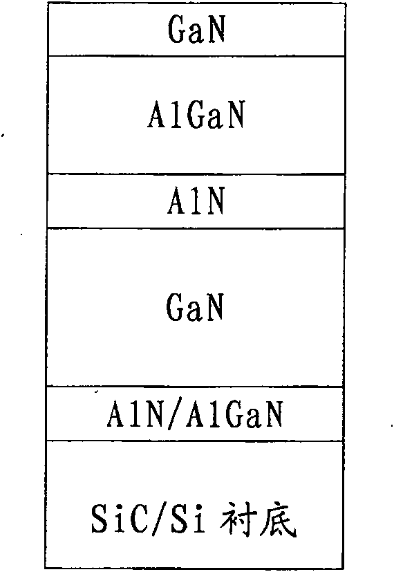
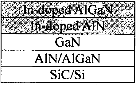
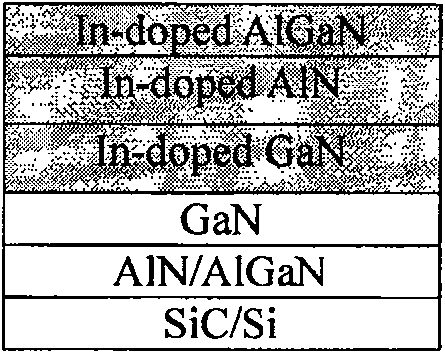
[0018] Figure 2-1 to Figure 2-7 These are several typical structures of indium-doped GaN HEMT materials grown by the technology of the present invention. Its growth equipment uses a metal-organic chemical vapor deposition (MOCVD) epitaxial growth system. The substrate for raw material growth is SiC or Si single crystal substrate. The growth atmosphere is trimethylgallium (TMGa), trimethylaluminum (TMAl ), trimethylindium (TMIn) and ammonia (NH 3 ) respectively as Ga, Al, In and N sources, with hydrogen (H 2 ) is the carrier gas, and the flow rate of trimethylindium (TMIn) is 0-10umol / min during the growth process. Below is Figure 2-1 to Figure 2-7 Growth steps and structural conditions of each structure shown:

[0019] diagram 2-1 To grow a layer of AlN or AlGaN nucleation layer on SiC / Si substrate, then grow GaN buffer layer and channel layer, then grow indi...


PUM

PropertyMeasurementUnit
thicknessaaaaaaaaaa
thicknessaaaaaaaaaa

Abstract

The invention discloses a method of increasing the properties of the gallium nitride-based transistor material and device with indium doping and applies in the field of making gallium nitride-based HEMT or HFET materials and devices. The method and process is to form the gallium nitride-based high electron mobility transistor or heterostructure field effect transistor materials on SiC or Si single crystal substrate grown by metal-organic chemical vapor deposition epitaxial growth system. After the AlN or AlGaN nucleating layer and the GaN buffer layer are grown on the SiC or Si single crystal substrate, a GaN channel layer, an AlN insert layer, an AlGaN barrier layer and a GaN capped layer are grown, and trimethyl indium is added in the growth atmosphere to do epitaxial growth with indium doping. The dislocation of the material or device made by the method of the invention is reduced greatly. The invention improves the interfacial smoothness, increases the electron mobility of the material, increases the growth window, ensures the material grow easier, improves the current collapse of the device, reduces the leakage current and increases transconductance and gain and increases the output power of microwave power devices.

Description

technical field [0001] The invention relates to a method for improving the material and device performance of gallium nitride (GaN)-based high electron mobility transistor (HEMT) or gallium nitride-based heterojunction field-effect transistor (HFET) by using indium doping technology, belonging to GaN-based Transistor material growth and device fabrication. Background technique [0002] Microwave devices such as AlGaN / GaN-based high electron mobility transistors (HEMTs) have properties such as high power density, high frequency and high breakdown voltage due to the wide band gap and intrinsic electronic polarity. Since the advent of the first AlGaN / GaN-based high electron mobility transistors, tremendous progress has been made in both material growth and device fabrication. The structure of GaN HEMT material is generally as follows figure 1 shown. At present, the method of growing this kind of material generally adopts MOCVD epitaxial growth system to carry out AlGaN / GaN h...

Claims


Application Information

Patent Timeline
Patent Type & Authority Patents(China)
IPC IPC(8): H01L21/335H01L21/205
Inventor 冯志红
Owner THE 13TH RES INST OF CHINA ELECTRONICS TECH GRP CORP
Why Eureka
Try Eureka