Device structure based on quasi-linear doping of III-nitride materials

A device structure, quasi-linear technology, applied in the direction of semiconductor devices, electrical components, diodes, etc., can solve the problems of poor F processing stability, quasi-linear doping difficulty, etc., to reduce difficulty, reduce implementation costs, and reduce current collapse. Effect

Active Publication Date: 2017-04-26
THE 13TH RES INST OF CHINA ELECTRONICS TECH GRP CORP
View PDF3 Cites 0 Cited by
  • Summary
  • Abstract
  • Description
  • Claims
  • Application Information

AI Technical Summary

Problems solved by technology

[0005] In order to solve the problems of the difficulty in achieving quasi-linear doping by ion implantation of III-nitride materials and the poor stability of F treatment, the present invention provides a device structure based on quasi-linear doping of III-nitride materials, which utilizes polarization engineering , using multiple trenching technology to achieve quasi-linear doping of III-nitride materials

Method used


Image

  • Device structure based on quasi-linear doping of III-nitride materials
  • Device structure based on quasi-linear doping of III-nitride materials
  • Device structure based on quasi-linear doping of III-nitride materials

Examples


Embodiment 1

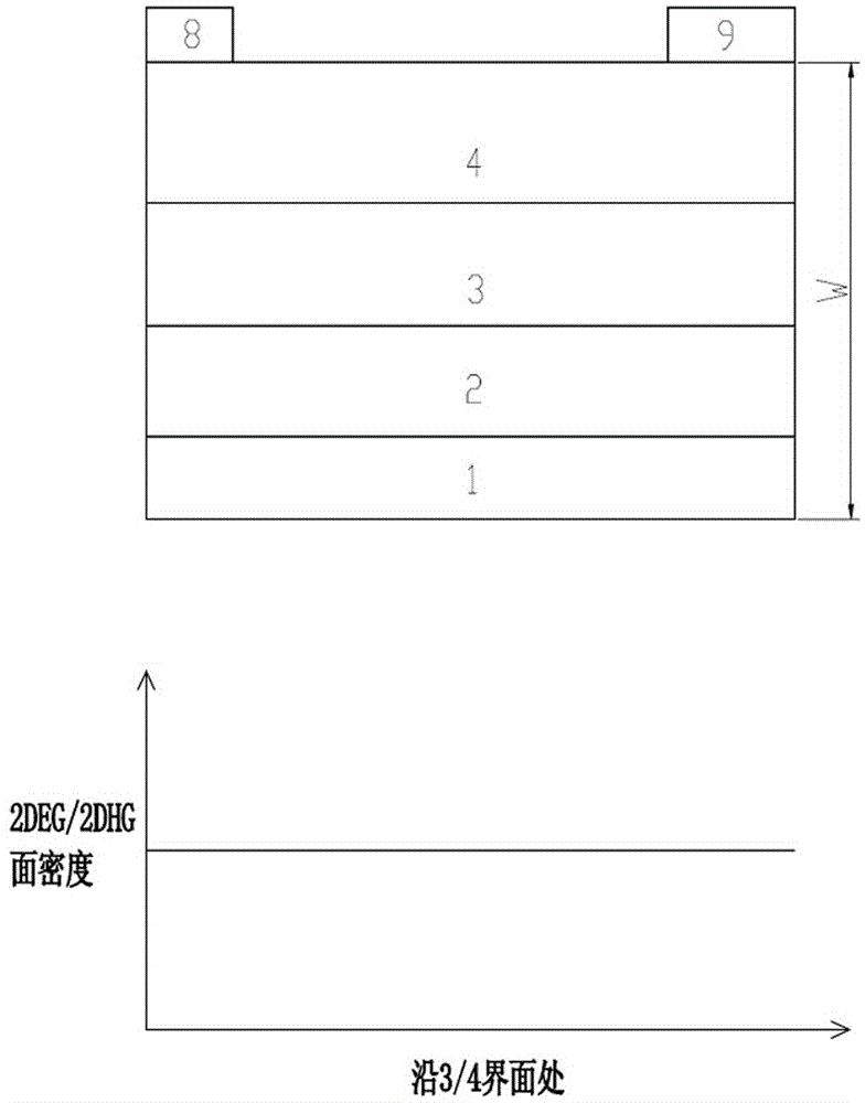
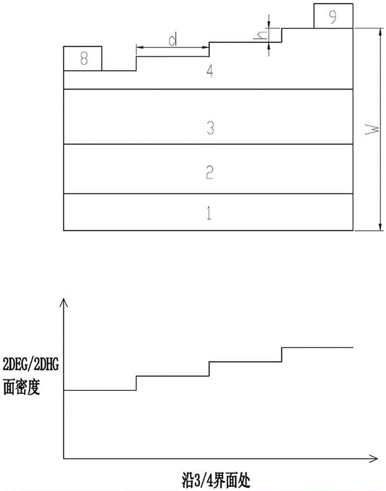
[0028] Depend on Figure 4 As can be seen, the quasi-linearly doped SBD device structure based on Group III nitride materials includes a substrate 1, a buffer layer 2, a channel layer 3 and a barrier layer 4 from bottom to top, and the barrier layer 4 An anode electrode 8 and a cathode electrode 9 are arranged at both ends of the upper surface; the upper surface of the barrier layer 4 increases stepwise, and the increasing direction is from the anode electrode 8 to the cathode electrode 9 . Because the changing direction of the incremental part should be gradually increasing from the low-potential electrode to the high-potential electrode under the reverse cut-off state of the device; 9 is a high potential voltage, so from Figure 4 It can be observed that the stepwise increase is from left to right.

[0029] In this embodiment, the incremental part starts from the anode electrode 8 at the left end of the barrier layer 4 and increases to the cathode electrode 9 at the right ...

Embodiment 2

[0039] Such as Image 6 It can be seen that, unlike Embodiment 1, part of the upper surface of the barrier layer 4 increases in steps. Depend on Image 6 It can be seen that the stepwise increasing direction is increasing from right to left, and the increasing direction is just opposite to that of Embodiment 1. The rule of the direction: in the reverse cut-off state of the device, gradually increase from the low-potential electrode to the high-potential electrode. In this embodiment, the stepwise increasing direction should be from right to left.

[0040] The difference between this embodiment and Embodiment 1 is that: 1) the stepwise increasing part occupies part of the upper surface of the barrier layer 4; 2) the height difference h between the steps is different; 3) the width d of each step is also 4) The height of the highest step is lower than the equal plane height W of the barrier layer 4 .

[0041] Substrate 1 is diamond in the present embodiment; Buffer layer 2 is ...

Embodiment 3

[0043] Such as Figure 8 As shown, the HEMT structure based on the quasi-linear doping of group III nitride materials includes a substrate 1, a buffer layer 2, a channel layer 3 and a barrier layer 4 from top to bottom; different from Embodiment 1, the The upper surface of the barrier layer 4 is provided with a source electrode 5 , a gate electrode 6 and a drain electrode 7 . The height of part of the upper surface of the barrier layer 4 increases stepwise, and this part is located between the gate electrode 6 and the drain electrode 7 on the barrier layer 4 , which is similar to the position of the second embodiment. The increasing direction is from the gate electrode 6 to the drain electrode 7, and here also follows the rules of the increasing direction: in the reverse cut-off state of the device, it gradually increases from the low potential electrode to the high potential electrode, and in the cut off state, the gate electrode 6 is applied with a low potential voltage, an...


PUM


Abstract

The invention discloses a quasi-linear doped device structure based on III-nitride materials, belonging to semiconductor high-frequency power devices and high-voltage devices, in particular to the high-voltage field of III-nitride devices. In the present invention, the bottom-up includes a substrate, a buffer layer, a channel layer and a barrier layer with electrodes on the upper surface, and the upper surface on the barrier layer is partially or fully stepped up; the increasing direction is: When the device is in the reverse cut-off state, the direction is from the low potential electrode to the high potential electrode. Compared with the conventional III-nitride device structure, the main innovation of the present invention is to realize the quasi-linear doping of the barrier layer channel through the trenching process, cleverly avoiding the second-implantation process of the III-nitride, and reducing the production cost. It also reduces the manufacturing cost of the device; and the quasi-linear doping of the present invention effectively reduces the original peak electric field, effectively increases the breakdown voltage of the device, and reduces current collapse.

Description

technical field [0001] The present invention relates to the field of semiconductor devices. Background technique [0002] Document 1 "Dependence of Breakdown Voltage on Drift Length and LinearDoping Gradients in SOI RESURF LDMOS Devices" (Shaoming Yang, Wenchin Tseng and Gene Sheu., The Ninth International Conference on Electronic Measurement & Instruments 2009, pp, 594-597) reported linear doping The device effectively improves the breakdown voltage of the device, and the impact of uniform doping and linear doping on the breakdown voltage is compared for example figure 1 shown. [0003] Document "High breakdown voltage AlGaN / GaN HEMT by employing selectivefluoride plasma treatment" (Young-Shil Kim, Jiyong Lim, O-Gyun Seok and Min-koo Han. Proceedings of the 23rd International Symposium on PowerSemiconductor Devices & IC's May 23-26, 2011 San Diego, CA, pp. 251-255) used F treatment to form a 2-Dimensional Electron Gas (2DEG) concentration difference, which effectively inc...

Claims


Application Information

Patent Timeline
Patent Type & Authority Patents(China)
IPC IPC(8): H01L29/06H01L29/778H01L29/872
CPCH01L29/0657H01L29/778H01L29/2003H01L29/66212H01L29/7786H01L29/872
Inventor 王元刚冯志红敦少博吕元杰张雄文房玉龙
Owner THE 13TH RES INST OF CHINA ELECTRONICS TECH GRP CORP
Why Eureka
Try Eureka