Memory device and operation method thereof

Active Publication Date: 2022-01-13
WINBOND ELECTRONICS CORP
View PDF0 Cites 0 Cited by
  • Summary
  • Abstract
  • Description
  • Claims
  • Application Information

AI Technical Summary

Benefits of technology

The disclosure is about a memory device with a pipeline structure that can reduce the time it takes to operate the device.

Problems solved by technology

The operation speed of dynamic random access memory (DRAM) is limited to its own accessing mechanism.
How to improve the accessing speed of DRAM is an important issue, especially for DRAM having an error-correcting code (ECC) circuit.
The ECC circuit may improve data reliability but may lead to an increase in column-to-column delay (tCCD) of DRAM.
Therefore, how to provide a memory device exhibiting high reliability and high speed is an important issue in the development of memory technology at present.

Method used


Image

  • Memory device and operation method thereof
  • Memory device and operation method thereof
  • Memory device and operation method thereof

Examples


Embodiment Construction

[0018]In order to make the disclosure more comprehensible, several embodiments are described below as examples of implementation of the disclosure. Moreover, elements / components / steps with the same reference numerals are used to represent the same or similar parts in the drawings and embodiments.

[0019]In the following embodiments, a dynamic random access memory (DRAM) is implemented as an example to illustrate a memory device and an operation method thereof provided by the disclosure. Nevertheless, types of the memory device are not limited by the disclosure.

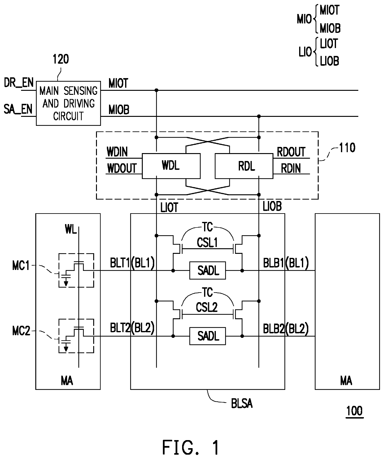
[0020]FIG. 1 is a schematic diagram of circuits of a memory device according to an embodiment of the disclosure. With reference to FIG. 1, a memory device 100 at least includes an input / output data latch circuit 110, a bit line sensing amplifier circuit BLSA, and a memory cell array MA. The memory cell array MA is formed by a plurality of memory cells arranged into an array. These memory cells are connected to a plurality of wor...


PUM


Abstract

A memory device and an operation method thereof are provided. The memory device includes an input / output data latch circuit and a bit line sensing amplifier circuit. The input / output data latch circuit is coupled between a main input / output line pair and a local input / output line pair. The local input / output line pair is coupled to a plurality of bit line pairs through the bit line sensing amplifier circuit. The memory device performs a two-stage operation to input or output data of a selected bit line pair among the bit line pairs. The selected bit line pair connects to the local input / output line pair only during one stage operation of the two-stage operation. Further, during the other stage operation of the two-stage operation, the data of the selected bit line pair latched in the input / output data latch circuit is transmitted to the main input / output line pair.

Description

BACKGROUNDTechnical Field[0001]The disclosure relates to a memory device, and more particularly, relates to a memory device providing improved accessing speed and an operation method thereof.Description of Related Art[0002]The operation speed of dynamic random access memory (DRAM) is limited to its own accessing mechanism. How to improve the accessing speed of DRAM is an important issue, especially for DRAM having an error-correcting code (ECC) circuit. The ECC circuit may improve data reliability but may lead to an increase in column-to-column delay (tCCD) of DRAM. Therefore, how to provide a memory device exhibiting high reliability and high speed is an important issue in the development of memory technology at present.SUMMARY[0003]The disclosure provides a memory device and an operation method thereof in which a pipeline structure is included, so that an operation cycle of the memory device is reduced.[0004]An embodiment of the disclosure provides a memory device including an inp...

Claims


Application Information

Patent Timeline
IPC IPC(8): G11C11/4091G11C11/4094G11C11/4096
CPCG11C11/4091G11C11/4096G11C11/4094G11C11/4076G11C11/4097G11C7/1039G11C2207/005
Inventor KADOWAKI, TAKUYA
Owner WINBOND ELECTRONICS CORP
Why Eureka
Try Eureka