Semiconductor device

a technology of semiconductor devices and dielectric devices, which is applied in the direction of semiconductor devices, semiconductor/solid-state device details, electrical apparatus, etc., can solve the problem of hard to increase the net die, and achieve the effect of suppressing the seam lateral migration, preventing the punching of the word lines, and reducing the parasitic capacitance between the bit line and the word lines

Pending Publication Date: 2022-01-13
SK HYNIX INC
View PDF3 Cites 6 Cited by
  • Summary
  • Abstract
  • Description
  • Claims
  • Application Information

AI Technical Summary

Benefits of technology

[0012]According to embodiments of the present disclosure, lateral migration of the seam may be suppressed by the liner material. Thus, punching of the word lines may be prevented.
[0013]According to embodiments of the present disclosure, a low-k material and an air gap are formed between the bit line and the word lines. Thus, parasitic capacitance between the bit line and the word lines may be reduced.

Problems solved by technology

Although the shrunken memory cell is supposed to lead to a decrease in parasitic capacitance (Cb) and an increase in capacitance, it is hard to increase the net die due to structural limitations to the memory cell.

Method used


Image

  • Semiconductor device
  • Semiconductor device
  • Semiconductor device

Examples


Embodiment Construction

[0022]Hereinafter, embodiments of the present disclosure are described with reference to schematic cross-sectional views, plan views, or block diagrams. Changes or modifications may be made to the views depending on manufacturing techniques and / or tolerances. Thus, embodiments of the disclosure are not limited to specific types as shown and illustrated herein but may rather encompass changes or modifications resultant from fabricating processes. For example, the regions or areas shown in the drawings may be schematically shown, and their shapes shown are provided merely as examples, rather than limiting the category or scope of the disclosure.

[0023]According to various embodiments of the present disclosure, it is possible to reduce parasitic capacitance while increasing memory cell density by vertically stacking memory cells.

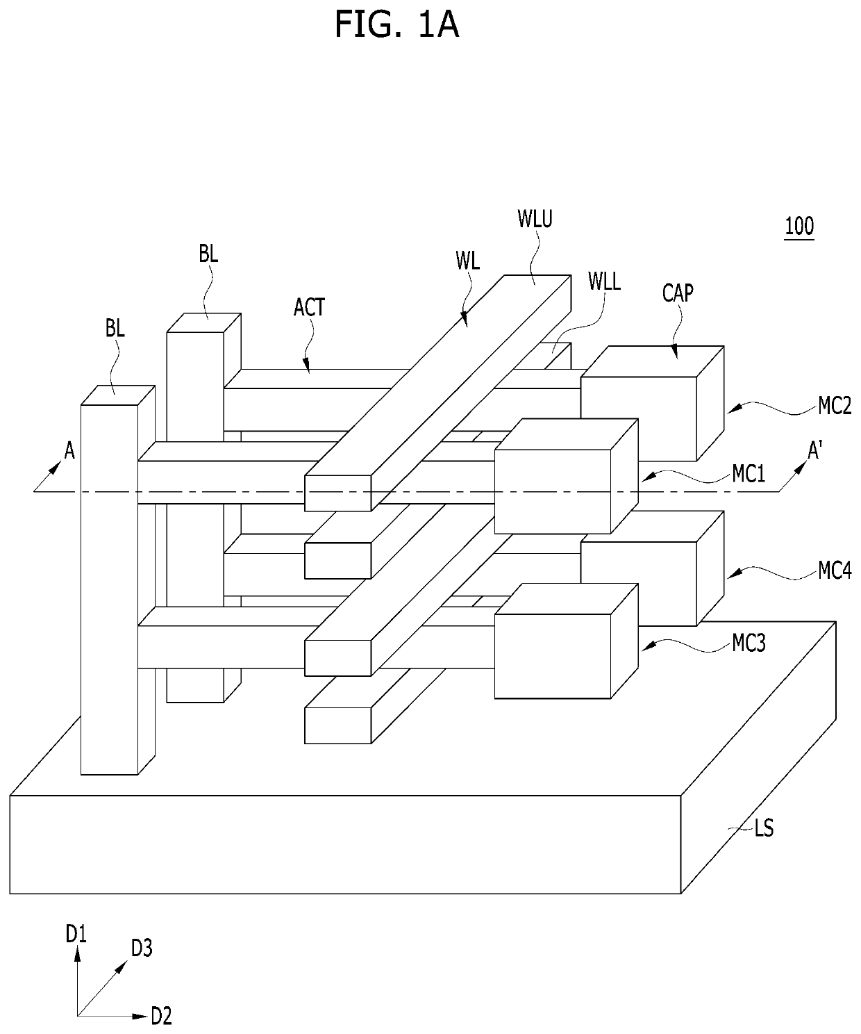
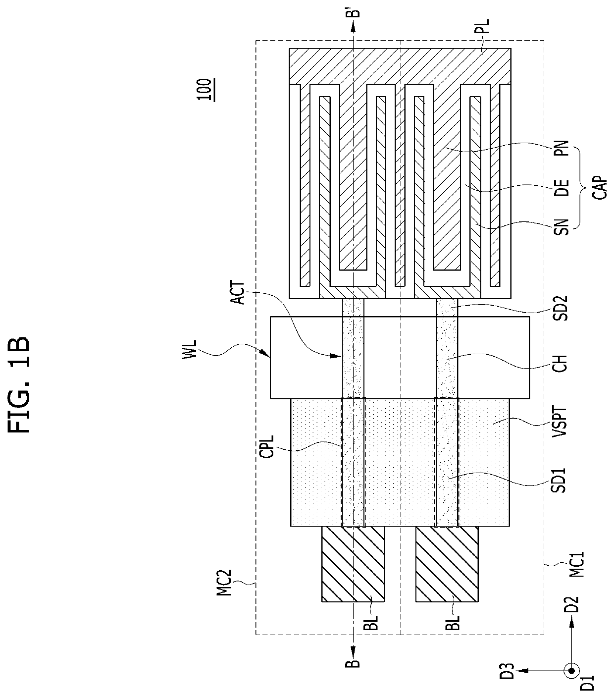
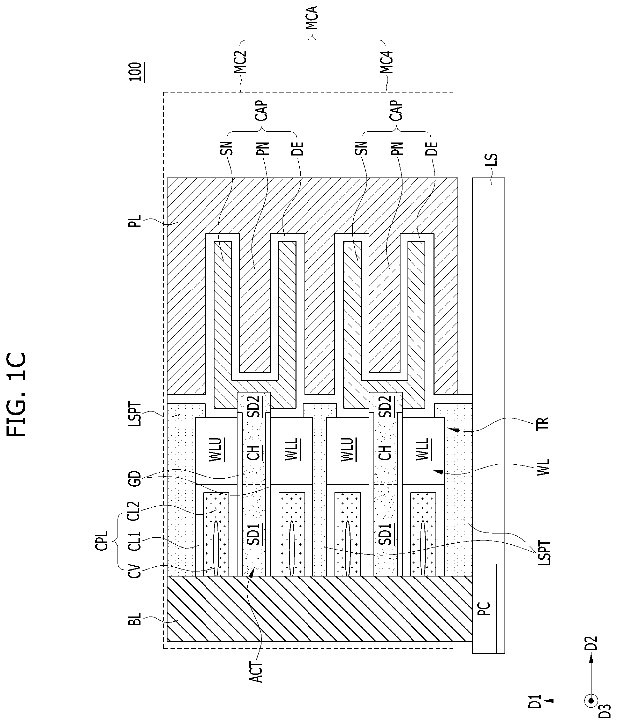
[0024]FIG. 1A is a perspective view illustrating a semiconductor device according to an embodiment of the present disclosure. FIG. 1B is a layout taken along li...


PUM

PropertyMeasurementUnit
dielectric constantaaaaaaaaaa

Abstract

According to the disclosure, highly integrated memory cells and a semiconductor device having the same are provided. According to an embodiment, a semiconductor device comprises a plurality of memory cells vertically stacked on a base substrate, each of the plurality of memory cells includes, a bit line vertically oriented from the base substrate, a capacitor horizontally spaced apart from the bit line, an active layer horizontally oriented between the bit line and the capacitor, a word line positioned on at least one of a top surface and bottom surface of the active layer and horizontally extending in a direction crossing the active layer, and a capping layer positioned between the word line and the bit line and including, at least, a low-k material and an air gap.

Description

CROSS-REFERENCE TO RELATED APPLICATIONS[0001]The present application claims priority to Korean Patent Application No. 10-2020-0083557, filed on Jul. 7, 2020, which is herein incorporated by reference in its entirety.BACKGROUND1. Field[0002]Embodiments of the disclosure relate to semiconductor devices and, more specifically, to memory cells and semiconductor devices including the memory cells.2. Description of the Related Art[0003]Recently, in order to increase the net die of the memory device, the memory cell has been continuously shrunken.[0004]Although the shrunken memory cell is supposed to lead to a decrease in parasitic capacitance (Cb) and an increase in capacitance, it is hard to increase the net die due to structural limitations to the memory cell.SUMMARY[0005]According to embodiments of the disclosure, highly integrated memory cells and a semiconductor device having the memory cells are provided.[0006]According to an embodiment, a semiconductor device comprises a plurality ...

Claims


Application Information

Patent Timeline
Patent Type & Authority Applications(United States)
IPC IPC(8): H01L27/108H01L27/13
CPCH01L27/10805H01L27/13H01L23/5329H10B12/30H01L29/78642H01L29/42392H01L27/0688H10B12/03H10B12/48
Inventor RYU, SEUNG WOOKSON, SUNG HUNLEE, KI HONG
Owner SK HYNIX INC
Why Eureka
Try Eureka