Embedded component structure and manufacturing method thereof

a technology of embedded components and manufacturing methods, applied in the field of embedded component structures, can solve the problems of increasing chip power consumption, waste heat accumulation, and ineffective and proper discharge of waste heat, and achieve the effect of effectively discharged waste heat and alleviating the problem of shortened life or even damage to the chip

Active Publication Date: 2022-01-20
UNIMICRON TECH CORP
View PDF0 Cites 2 Cited by
  • Summary
  • Abstract
  • Description
  • Claims
  • Application Information

AI Technical Summary

Benefits of technology

[0005]The disclosure provides an embedded component structure and a manufacturing method thereof, which may effectively discharge the waste heat to alleviate the problem of shortened life or even damage to the chip due to overheating.

Problems solved by technology

However, since the embedded chip is usually surrounded by a material (such as resin) with poor thermal conductivity, waste heat often cannot be discharged effectively and properly.
In addition, with the improvement of chip performance, power consumption of the chip also increases, which will make the problem of waste heat accumulation of the chip more obvious.
Furthermore, when the chip is in operation, a large amount of heat is easily produced.
If the heat is not properly discharged, it will easily shorten life or even damage the chip due to high temperature.
Therefore, how to effectively discharge the waste heat to alleviate the problem of shortened life or even damage to the chip due to overheating has become a great challenge for researchers in the art.

Method used


Image

  • Embedded component structure and manufacturing method thereof
  • Embedded component structure and manufacturing method thereof
  • Embedded component structure and manufacturing method thereof

Examples


Embodiment Construction

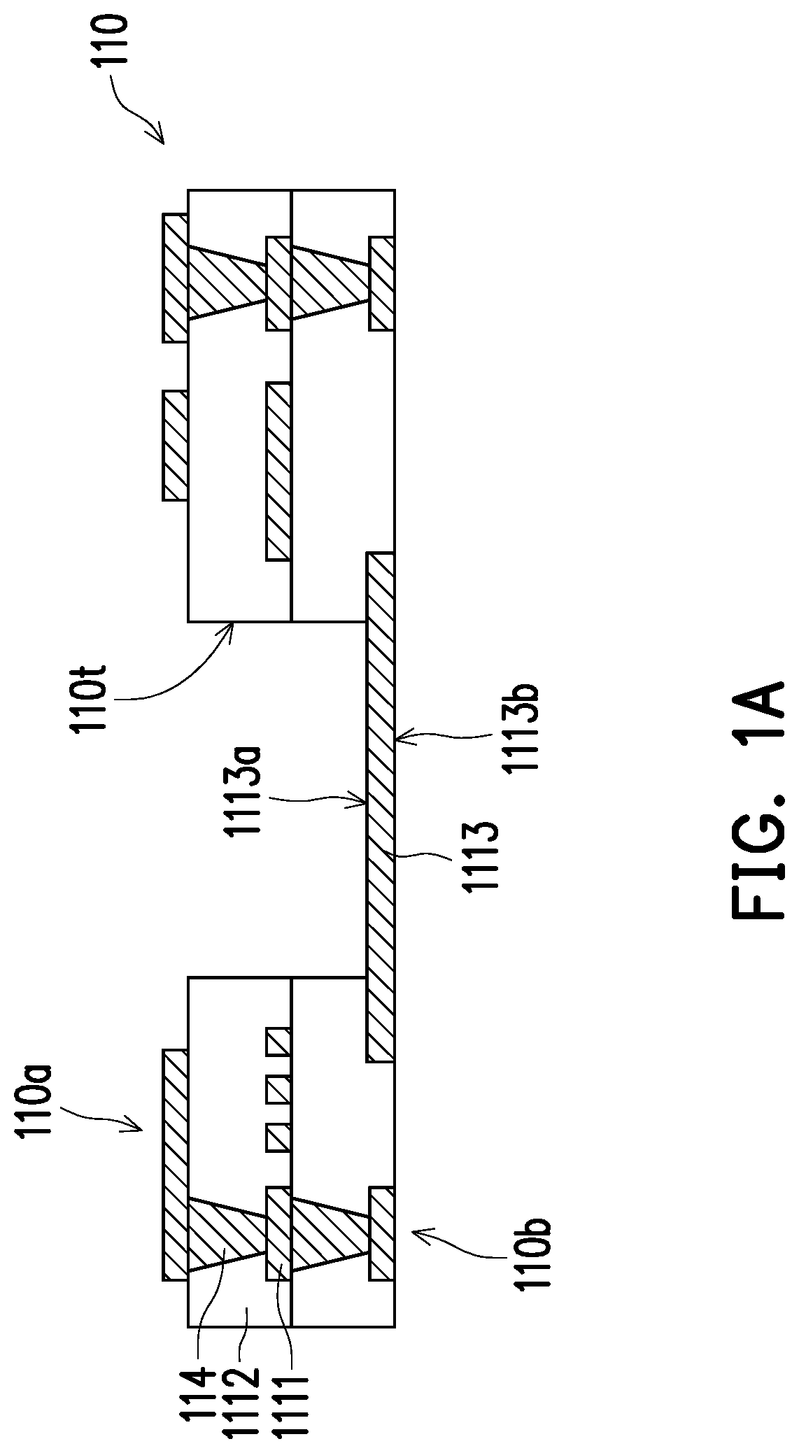
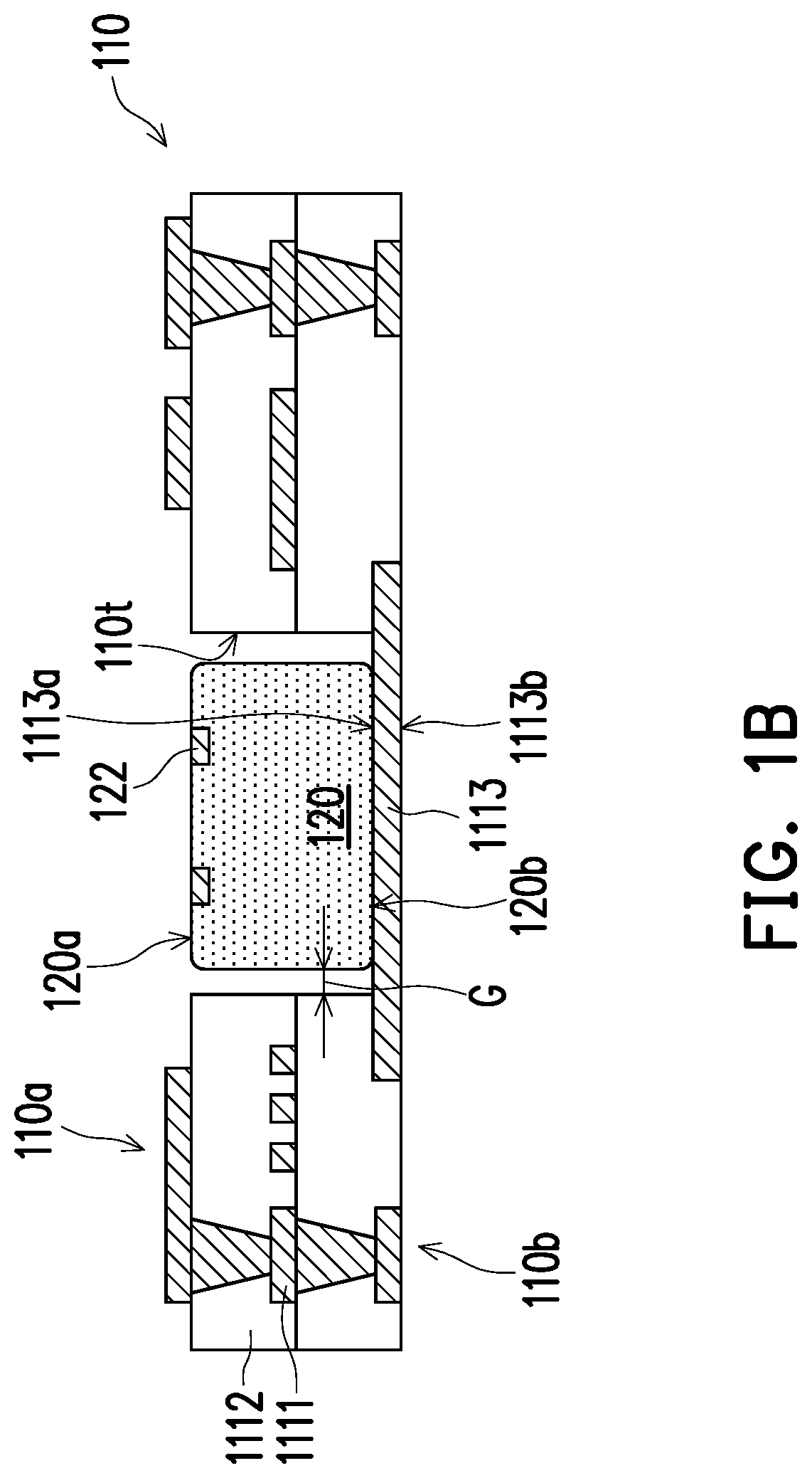
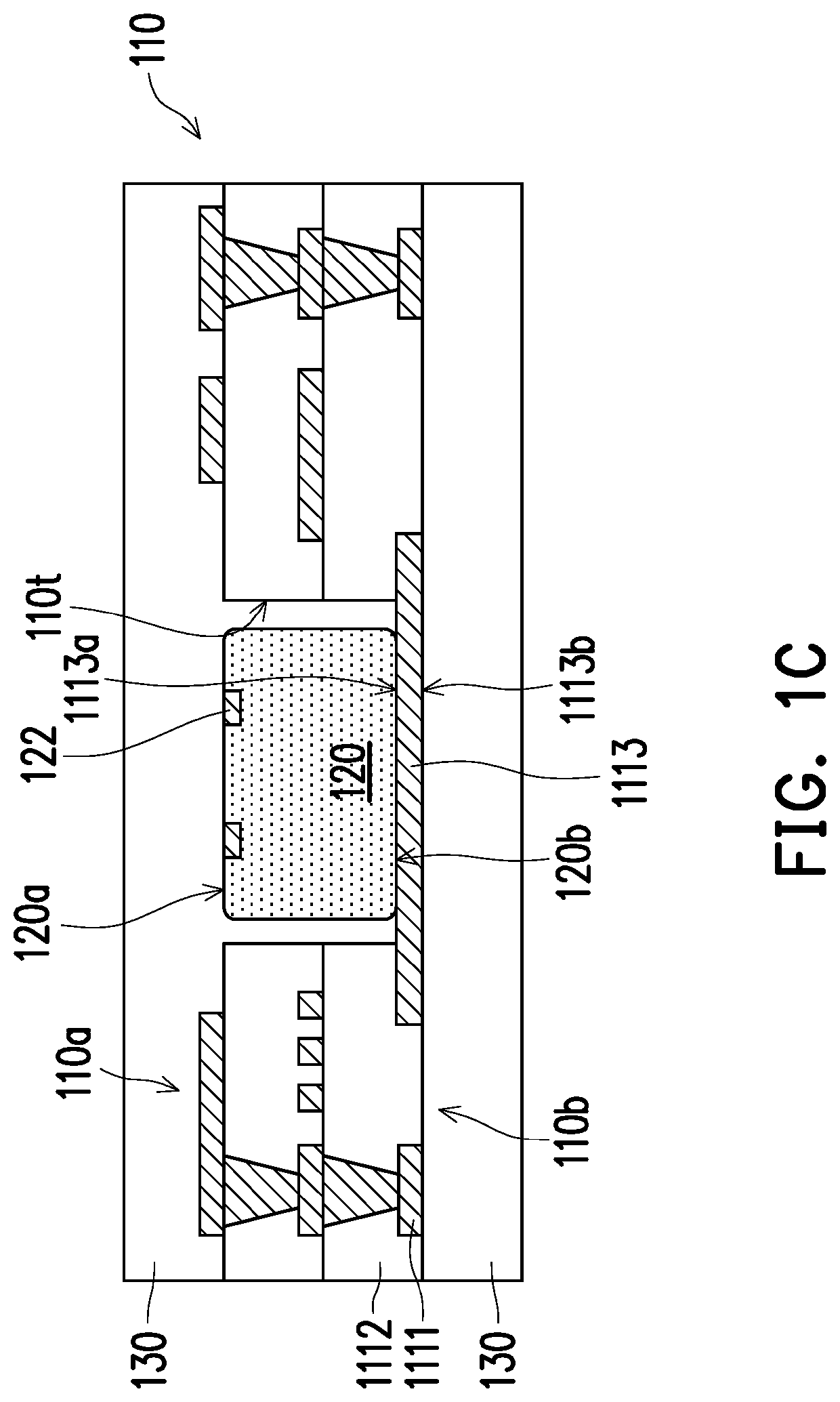
[0035]The foregoing and other technical content, features, and effects of the disclosure can be clearly presented below in detailed description with reference to embodiments of the accompanying drawings. The directional terms mentioned herein, like “above”, “below”, “front”, “back”, “left”, and “right”, refer to the directions in the accompanying drawings. Therefore, the directional terms are only used for illustration instead of limiting the disclosure.

[0036]In the detailed description of the embodiments, the terms, like “first”, “second”, and “third”, may be used for describing different elements. The terms are merely used for distinguishing between the elements, but these elements should not be limited by these terms in a structure. For example, a first element may be referred to as a second element, moreover, similarly, the second element may be referred to as the first element without departing from the protection scope of the ideas of the disclosure. In addition, in the manufa...


PUM


Abstract

An embedded component structure includes a circuit board, a chip, and a heat dissipation element. The chip is embedded in the circuit board. The heat dissipation element surrounds the chip. The chip, the circuit board, and the heat dissipation element are electrically connected. The heat dissipation element includes a first part, a second part, and a third part located between the first part and the second part. The first part is in direct contact with a side wall of the chip. The second part is a ground terminal. A method for manufacturing an embedded component structure is also provided.

Description

CROSS-REFERENCE TO RELATED APPLICATION[0001]This application claims the priority benefit of Taiwan application serial no. 109123678, filed on Jul. 14, 2020. The entirety of the above-mentioned patent application is hereby incorporated by reference herein and made a part of this specification.BACKGROUND OF THE DISCLOSURE1. Field of the Disclosure[0002]The disclosure relates to an electronic component and a manufacturing method thereof, and in particular, to an embedded component structure and a manufacturing method thereof.2. Description of Related Art[0003]In recent years, an embedded chip is usually used to reduce a carrying area on a circuit board in an electronic product. However, since the embedded chip is usually surrounded by a material (such as resin) with poor thermal conductivity, waste heat often cannot be discharged effectively and properly. In addition, with the improvement of chip performance, power consumption of the chip also increases, which will make the problem of ...

Claims


Application Information

Patent Timeline
Patent Type & Authority Applications(United States)
IPC IPC(8): H05K1/02H01L23/498H01L23/367H01L21/48
CPCH05K1/0207H01L23/49838H01L23/49822H01L21/4882H01L21/4857H01L23/3675H01L23/367H01L23/3677H01L23/3735H01L23/3736H01L23/552H01L21/4871H01L23/13H05K1/182H05K1/0203
Inventor CHEN, YU-SHEN
Owner UNIMICRON TECH CORP
Why Eureka
Try Eureka