Semiconductor device

a semiconductor and reverse conducting technology, applied in the direction of semiconductor devices, basic electric elements, electrical equipment, etc., can solve the problems of insufficient boundary region security, recovery loss cannot be reduced, recovery loss increases, etc., and achieve the effect of reducing recovery loss

Pending Publication Date: 2022-04-07
MITSUBISHI ELECTRIC CORP
View PDF7 Cites 2 Cited by
  • Summary
  • Abstract
  • Description
  • Claims
  • Application Information

AI Technical Summary

Benefits of technology

[0005]It is an object of the technique of the present disclosure to reduce recovery loss while an operating region is secured in an RC-IGBT.

Problems solved by technology

The RC-IGBT has high hole injection efficiency in an IGBT cell, and thus causes a problem in that recovery loss increases due to hole injection from an IGBT region to a diode region.
Unfortunately, the boundary region does not operate as an IGBT or a diode, and thus serves an invalid region that is not actively involved in energization operation.
This causes a problem in that a sufficient boundary region cannot be secured and recovery loss cannot be reduced to secure an effective operating region necessary for securing a sufficient energizing capacity in a limited element region.

Method used


Image

  • Semiconductor device
  • Semiconductor device
  • Semiconductor device

Examples


Embodiment Construction

A. First Preferred Embodiment

[0033]

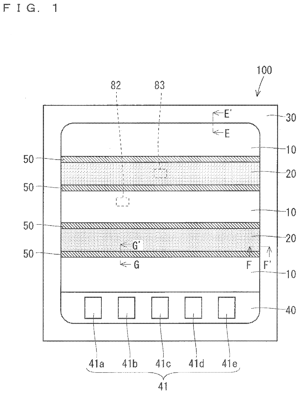
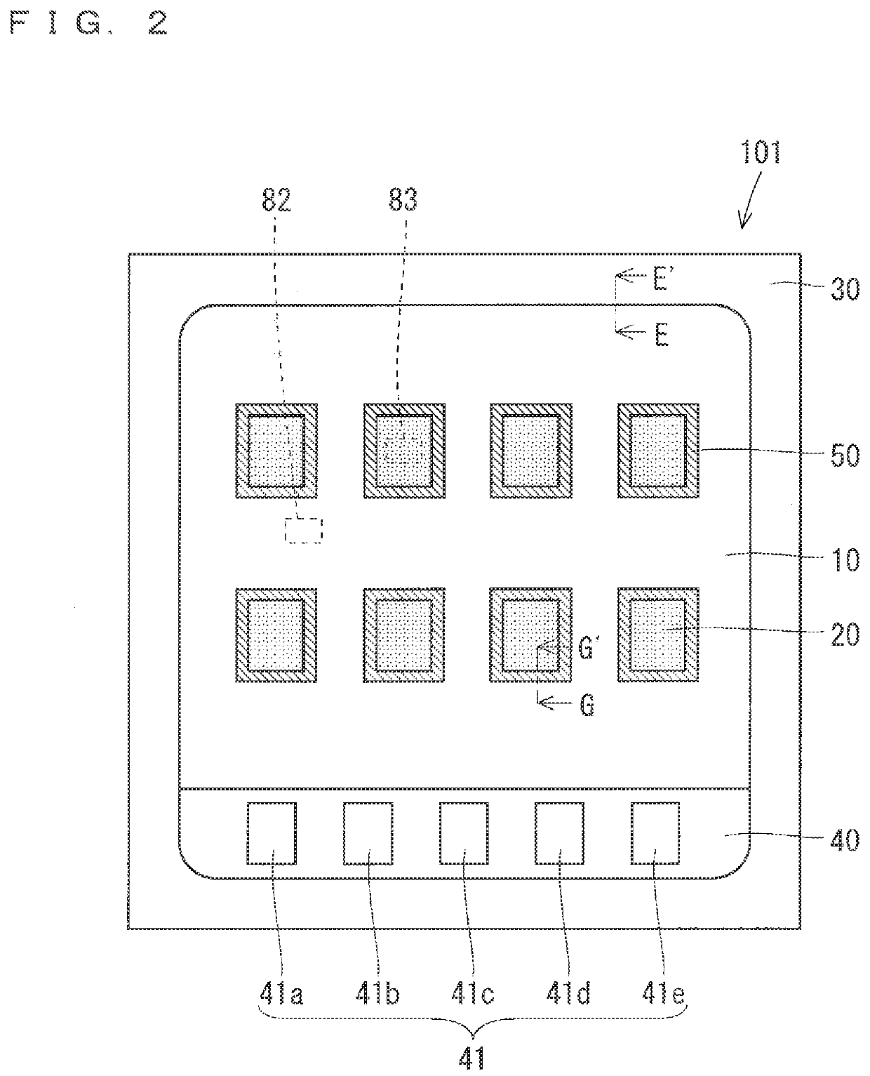
[0034]FIG. 1 is a plan view of a reverse conducting IGBT (RC-IGBT) 100 that is a semiconductor device of a first preferred embodiment. FIG. 2 is a plan view of an RC-IGBT 101 that is a semiconductor device of the first preferred embodiment, being different in structure from the RC-IGBT 100.

[0035]The RC-IGBT 100 has an IGBT region 10 and a diode region 20 arranged in stripe shape, and thus is also referred to as a “stripe type”. The RC-IGBT 101 has a structure in which an IGBT region 10 surrounds a plurality of diode regions 20, and thus is also referred to as an “island type”.

[0036]

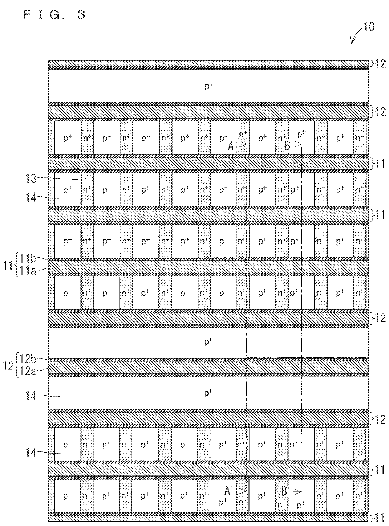
[0037]With reference to FIG. 1, a planar structure of the RC-IGBT 100 of a stripe type will be described, The RC-IGI3T 100 includes the IGBT region 10, the diode region 20, a terminal region 30, a pad region 40, and a boundary region 50. The RC-IGBT 100 includes the IGBT region 10 and the diode region 20 that are disposed with the. boundary region 50 interposed therebetw...


PUM

PropertyMeasurementUnit
distanceaaaaaaaaaa
conductivityaaaaaaaaaa
conductivity typeaaaaaaaaaa

Abstract

In plan view of an RC-IGBT, a boundary region has an occupancy rate of an n+-type source layer per unit area, the occupancy rate being smaller than an occupancy rate of the n+-type source layer per unit area in an IGBT region, and the boundary region has an occupancy rate of a p+-type contact layer per unit area, the occupancy rate being smaller than an occupancy rate of the p+-type contact layer per unit area in an IGBT region.

Description

BACKGROUND OF THE INVENTIONField of the Invention[0001]The present disclosure relates to a reverse conducting semiconductor device (RC-IGBT) in which a freewheeling diode and an insulated gate bipolar transistor (IGBT) are installed side by side.DESCRIPTION OF THE BACKGROUND ART[0002]The RC-IGBT has high hole injection efficiency in an IGBT cell, and thus causes a problem in that recovery loss increases due to hole injection from an IGBT region to a diode region.[0003]To address this problem, a boundary region is conventionally provided between the IGBT region and the diode region with a structure in which a collector layer is disposed directly under a diode cell (e.g., Japanese Patent Application Laid-Open No. 2018-073911).[0004]Unfortunately, the boundary region does not operate as an IGBT or a diode, and thus serves an invalid region that is not actively involved in energization operation. This causes a problem in that a sufficient boundary region cannot be secured and recovery l...

Claims


Application Information

Patent Timeline
Patent Type & Authority Applications(United States)
IPC IPC(8): H01L29/739H01L29/06H01L29/10
CPCH01L29/7394H01L29/1095H01L29/0696H01L29/0692H01L29/8613H01L29/407H01L29/7397H01L29/0834H01L29/0619H01L29/0638H01L29/4238
Inventor SONEDA, SHINYAHARADA, KENJIOTSUKA, KAKERU
Owner MITSUBISHI ELECTRIC CORP
Why Eureka
Try Eureka