Port processing method

Pending Publication Date: 2022-06-02
AMOLOGIC (SHANGHAI) CO LTD
View PDF0 Cites 0 Cited by
  • Summary
  • Abstract
  • Description
  • Claims
  • Application Information

AI Technical Summary

Benefits of technology

The present invention provides a method for enhancing the electrostatic discharge protection and overstress protection capabilities of contact cores and signal cores in a port processing device without adding extra cost. The method includes changing the signal layout of the contact cores and signal cores by disposing contact elastic pieces in a central portion of each contact core and signal core, extending the length of each contact core outwards, or adjusting the signal spacing between them. The method is simple and cost-effective.

Problems solved by technology

For example, when a human body contacts the port of the electronic product, electrostatic current will generate, and a short-term overvoltage or overcurrent phenomenon will occur when the contact is not made through the device, leading to ESD / EOS issue.
EOS issue is quite common in consumer electronics, and damage from this EOS issue is also very serious, which may damage CPU pins and they may be rendered useless, or may completely damage a certain module of the CPU and cause the entire system to fail to work.
The TV series, set-top box series and speaker series products used have similar problems, and this problem may even has become a bottleneck for customer after-sales quality.
However, another consideration which should be taken into account is cost.
Cost is linearly increased after a series of ESD protection measures are added, which may in turn bring rising costs in this industry.
When the two of above-mentioned wire cores are in contact with each other, issues regarding contact between two wire cores left and right, up and down may occur.
However, if two adjacent wire cores are designed to be very close to each other, signal mixing may occur.

Method used


Image

  • Port processing method
  • Port processing method
  • Port processing method

Examples


Embodiment Construction

[0028]The technical solution set forth in the embodiments of the present invention will now be described clearly and fully hereinafter with reference to the accompanying drawings of the embodiments of the present invention. Obviously, such embodiments provided in the present invention are only part of the embodiments instead of all embodiments. It should be understood that all the other embodiments obtained from the embodiments set forth in the present invention by one skilled in the art without any creative work fall within the scope of the present invention.

[0029]Notably, the embodiments set forth in the present invention and features of the embodiments may be combined in any suitable manner.

[0030]The present invention will be described hereinafter with reference to the accompanying drawings and particular embodiments, but the invention is not limited thereto.

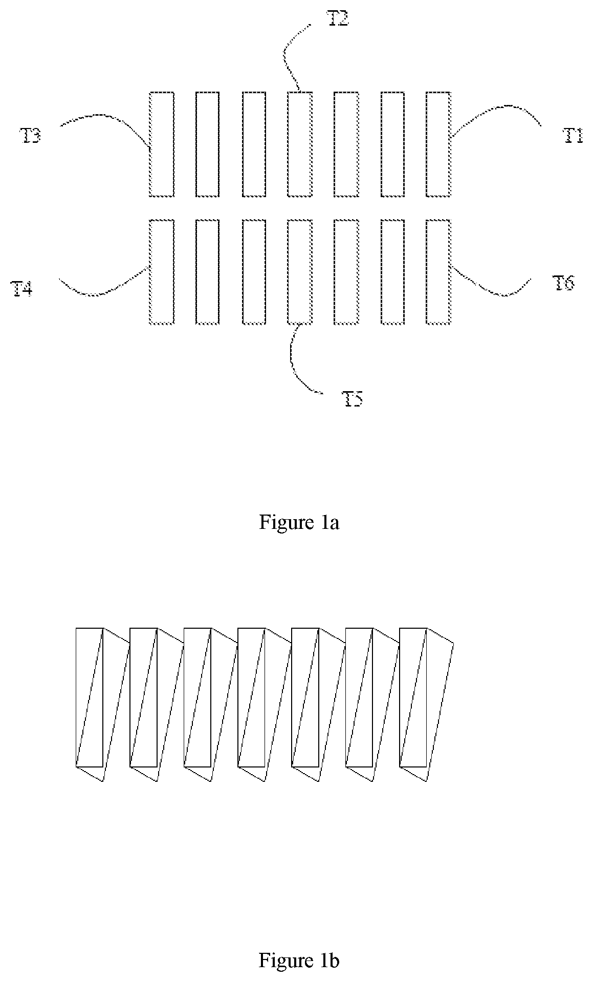
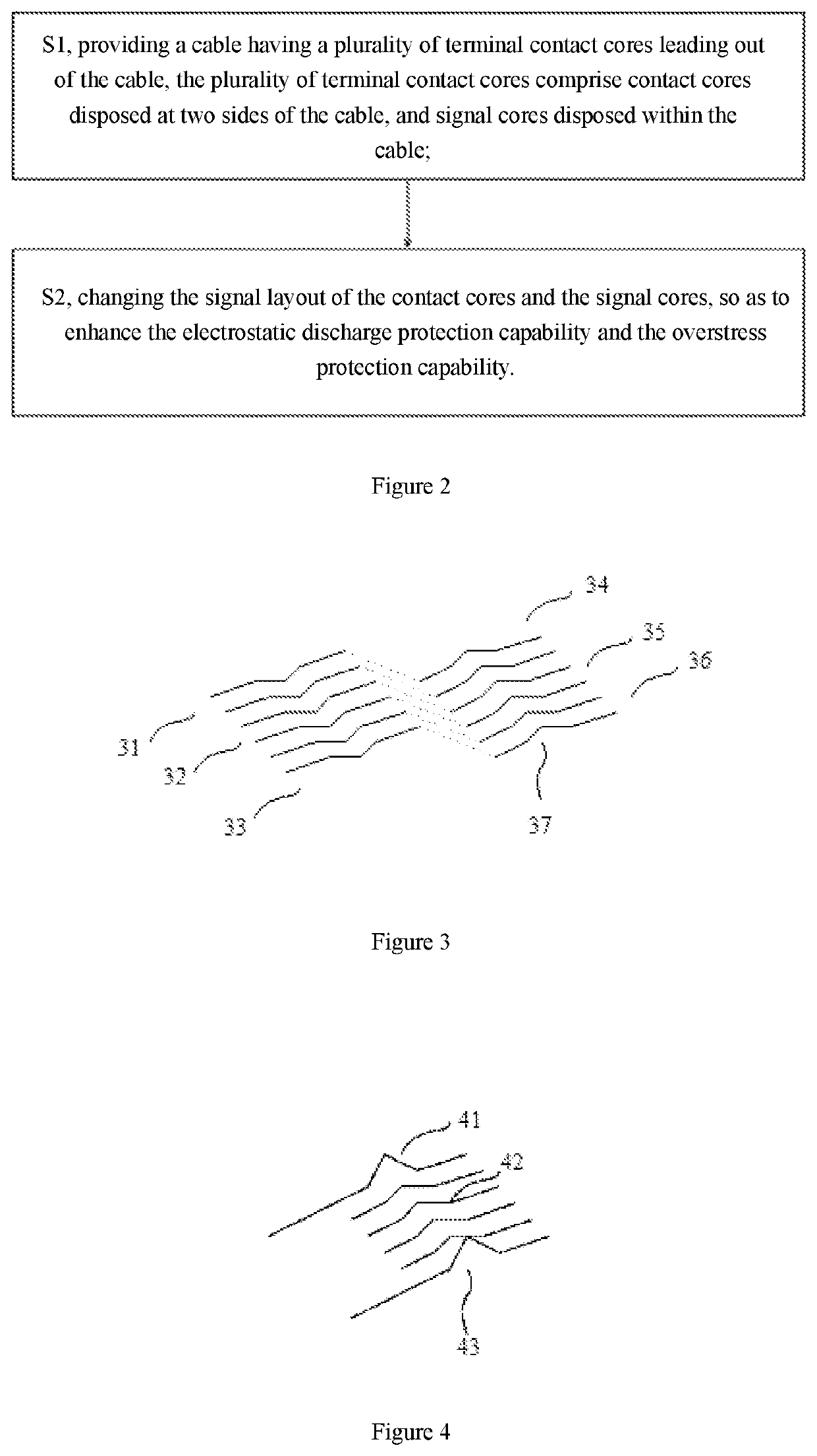
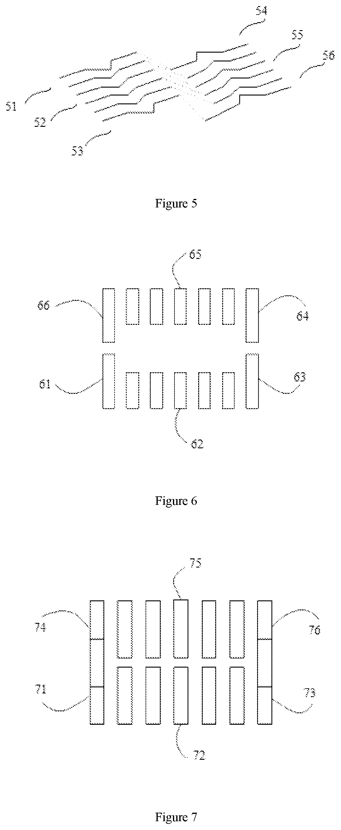
[0031]In the prior art, when it comes to the cause for EOS / ESD, three elements are key drivers for EOS / ESD damage, namely, ...


PUM


Abstract

A port processing method, used to enhance an electrostatic discharge protection capability and an overstress protection capability. The method comprises: step S1, providing a cable having a plurality of terminal contact cores leading out of the cable, the plurality of terminal contact cores comprising contact cores disposed at two sides of the cable, and signal cores disposed within the cable; and S2, changing the signal layout of the contact cores and the signal cores, so as to enhance the electrostatic discharge protection capability and the overstress protection capability. The method for changing the signal layout comprises: using the contact cores as a signal ground, and disposing a contact spring plate at a middle portion of each of the contact cores and each of the signal cores; and extending lengths of the contact cores outward.

Description

BACKGROUND OF THE INVENTION1. Field of the Invention[0001]The invention relates to the technical field of electrostatic protection and overvoltage protection, in particular to a port processing method.2. Description of the Related Art[0002]With the development of electronic products, ESD (Electrostatic Discharge) / ESD (Electrical Overstress) occurred on the electronics is a major concern for those in this industry. Many product manufacturers and chip solution manufacturers are working hard to solve the ESD / EOS issue caused by external factors. For example, when a human body contacts the port of the electronic product, electrostatic current will generate, and a short-term overvoltage or overcurrent phenomenon will occur when the contact is not made through the device, leading to ESD / EOS issue. EOS issue is quite common in consumer electronics, and damage from this EOS issue is also very serious, which may damage CPU pins and they may be rendered useless, or may completely damage a cer...

Claims


Application Information

Patent Timeline
IPC IPC(8): H01R43/00H01R13/648H01R13/02
CPCH01R43/00H01R13/02H01R13/6485H01R13/648H05F3/04H01R13/26
Inventor LIU, YONGZHANG, KUNHUANG, MINJUN
Owner AMOLOGIC (SHANGHAI) CO LTD
Why Eureka
Try Eureka