
Protection device and control circuit for a semiconductor switch and method for controlling a semiconductor switch

a control circuit and semiconductor technology, applied in electronic switching, electrical equipment, pulse techniques, etc., can solve problems such as overvoltage across the output terminals of semiconductors

Pending Publication Date: 2022-07-07
ROBERT BOSCH GMBH
View PDF3 Cites 0 Cited by
  • Summary
  • Abstract
  • Description
  • Claims
  • Application Information

AI Technical Summary

Benefits of technology

The present invention provides a protection device for a semiconductor switch that takes into account the capacitive properties of a component for detecting overvoltages. This allows reliable and quick detection of overvoltages at the semiconductor switching element and the introduction of suitable countermeasures in good time to prevent damage or premature ageing. The integrator can comprise a capacitor, which enables simple integration of quantities of charge.

Problems solved by technology

In this case, during opening of the switching elements, in particular of a semiconductor switching element, overvoltages may result across the output terminals of the semiconductor switch owing to leakage inductances or the like.

Method used


Image

  • Protection device and control circuit for a semiconductor switch and method for controlling a semiconductor switch
  • Protection device and control circuit for a semiconductor switch and method for controlling a semiconductor switch

Examples


Embodiment Construction

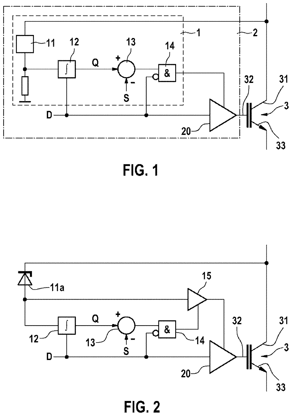
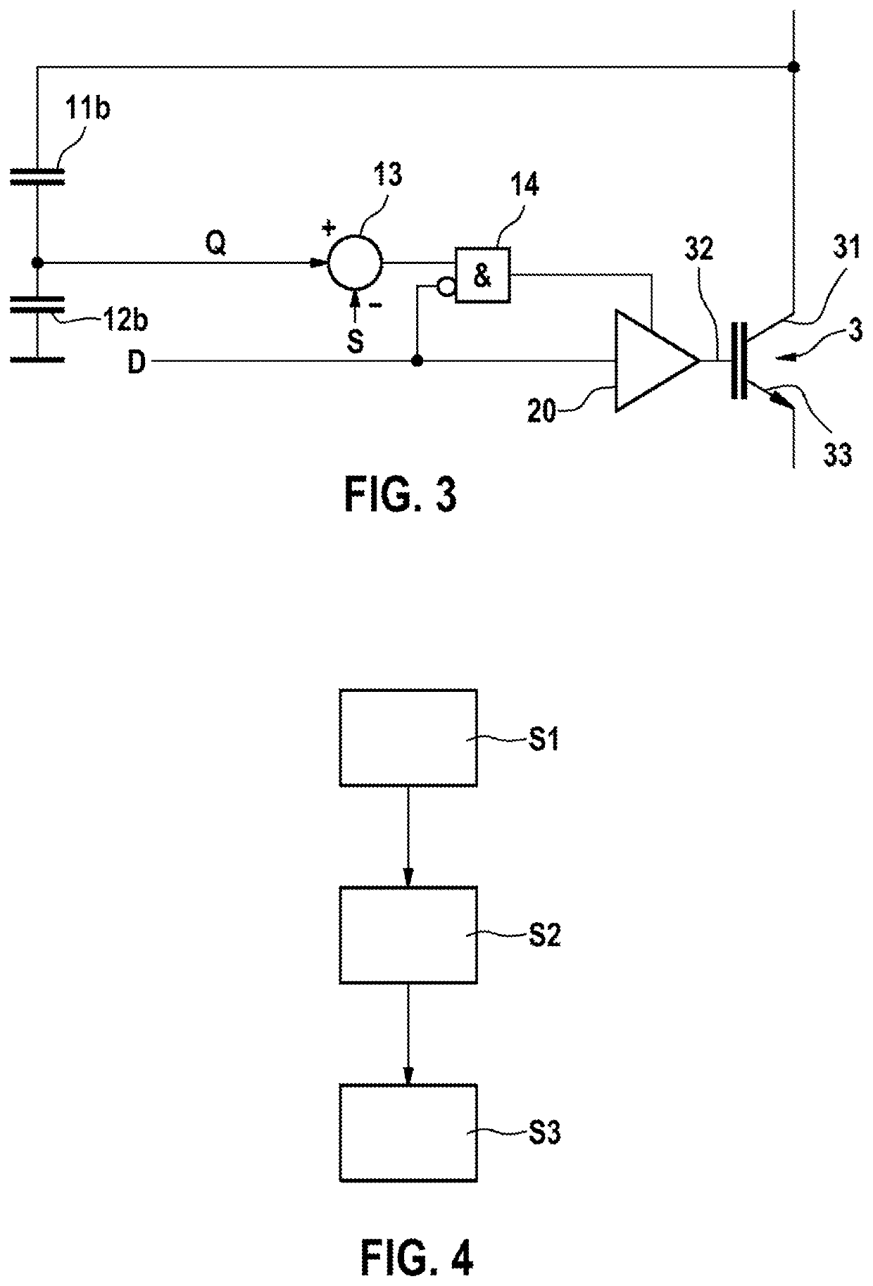
[0029]FIG. 1 shows a schematic illustration of a basic circuit diagram of a control circuit 2 for a semiconductor switch 3. The control circuit 2 comprises a driver circuit 20 for driving the gate 32 of the semiconductor switch 3. The driver circuit 20, for this purpose, receives a control signal D, amplifies this control signal D and, corresponding to the control signal D, controls the gate 32 of the semiconductor switch 3. In this way, the electrical connection between an input terminal 31 and an output terminal 33 of the semiconductor switch 3 can be opened or closed. For example, the semiconductor switch 3 may be a MOSFET or an insulated-gate bipolar transistor (IGBT). In principle, any other desired semiconductor switches are of course also possible. For example, the semiconductor switch 3 may be a semiconductor switch of a power stage, such as, for example, a power converter or the like. If the electrical connection between the input terminal 31 and the output terminal 33 of t...


PUM

PropertyMeasurementUnit
chargeaaaaaaaaaa
junction capacitanceaaaaaaaaaa
electrical voltageaaaaaaaaaa

Abstract

The invention relates to a protection for a semi-conductor switch against over voltages. A capacitive element is provided on an inlet connection of the semi-conductor switch. The load amount, which flows into said capacitive element, is integrated in order to trigger a protection function when a threshold value is exceeded.

Description

BACKGROUND OF THE INVENTION[0001]The present invention relates to a protection device for a semiconductor switch and to a control circuit for a semiconductor switch. In addition, the present invention relates to a method for controlling a semiconductor switch. In particular, the present invention relates to the protection of a semiconductor switch from overvoltages.[0002]The use of semiconductor switches as switching elements is gaining increasing importance. In this case, during opening of the switching elements, in particular of a semiconductor switching element, overvoltages may result across the output terminals of the semiconductor switch owing to leakage inductances or the like. In order to avoid any damage to the semiconductor switch as a result of such overvoltages, suitable overvoltage protection needs to be provided. Such overvoltage protection is known, for example, under the term “active clamping”.[0003]The document DE 10 2013 202 641 A1 discloses overvoltage protection ...

Claims


Application Information

Patent Timeline
Patent Type & Authority Applications(United States)
IPC IPC(8): H03K17/081
CPCH03K17/081H03K17/0828H03K17/168H03K17/165
Inventor SINN, PETERBRUCKHAUS, TIMRICHTER, TOBIAS
Owner ROBERT BOSCH GMBH
Learn More