Semiconductor devices including separation structure

Pending Publication Date: 2022-07-14
SAMSUNG ELECTRONICS CO LTD
View PDF0 Cites 0 Cited by
  • Summary
  • Abstract
  • Description
  • Claims
  • Application Information

AI Technical Summary

Benefits of technology

[0004]Some example embodiments of the inventive concepts provide semiconductor devices having excellent electrica

Problems solved by technology

In accordance with high integration of a semiconductor device, electrically separating a plurality of elements becomes mor

Method used


Image

  • Semiconductor devices including separation structure
  • Semiconductor devices including separation structure
  • Semiconductor devices including separation structure

Examples


Example

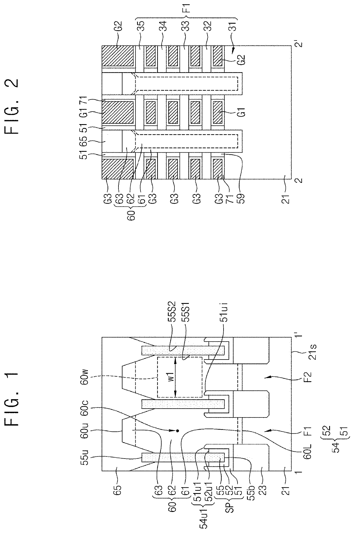
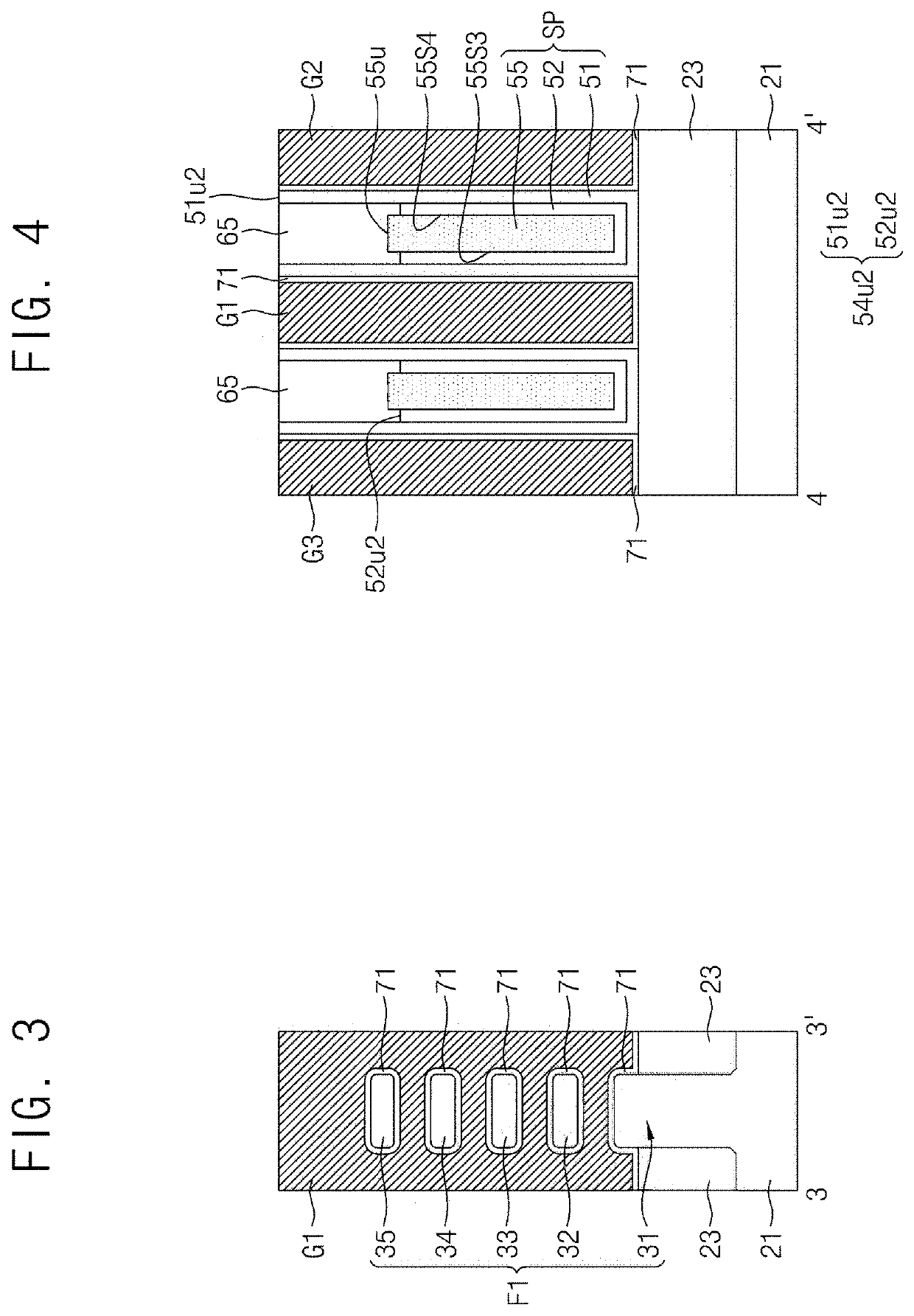
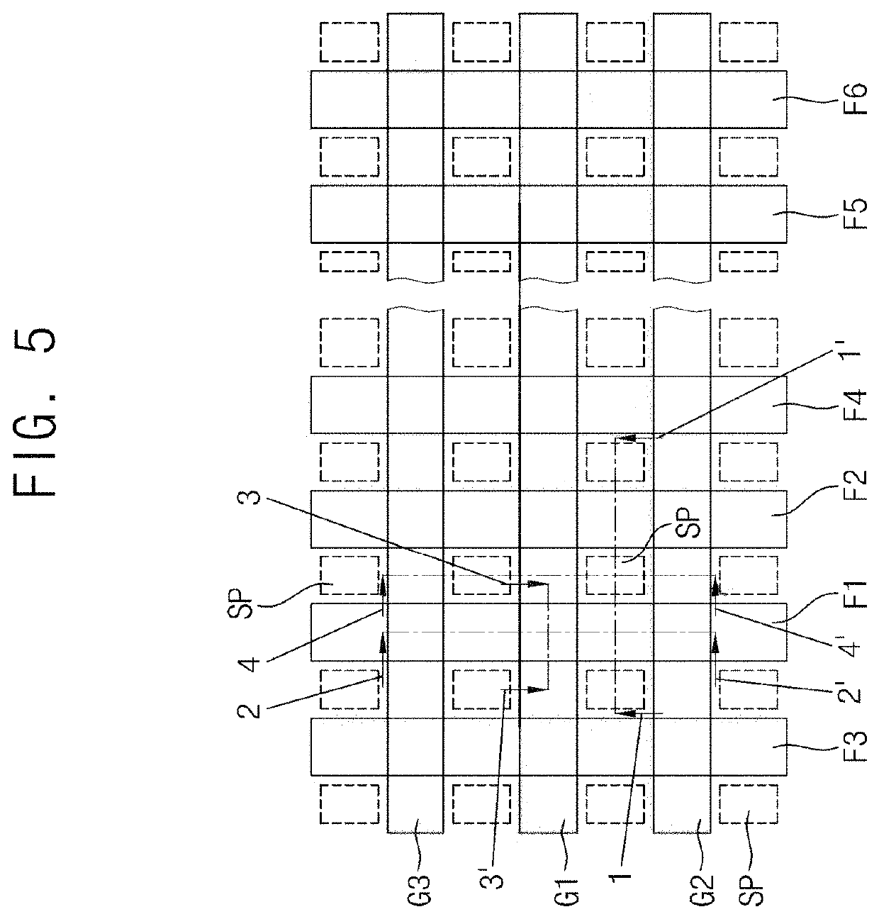
[0012]FIGS. 1, 2, 3, and 4 are cross-sectional views explaining semiconductor devices according to some example embodiments of the inventive concepts. FIG. 5 is a layout of semiconductor devices according to some example embodiments of the inventive concepts. FIG. 1 may be a cross-sectional view taken along line 1-1′ in FIG. 5. FIG. 2 may be a cross-sectional view taken along line 2-2′ in FIG. 5. FIG. 3 may be a cross-sectional view taken along line 3-3′ in FIG. 5. FIG. 4 may be a cross-sectional view taken along line 4-4′ in FIG. 5. In some example embodiments, semiconductor devices according to some example embodiments of the inventive concepts may include a multi-bridge channel transistor such as MBCFET, a fin field effect transistor (FinFET), a nanowire transistor, a vertical transistor, a recess channel transistor, a 3-D transistor, a planar transistor, or a combination thereof.

[0013]Referring to FIG. 1, a semiconductor device according to some example embodiments of the invent...


PUM


Abstract

A semiconductor device includes a plurality of active regions on a substrate. A gate electrode is on, and intersects, the active regions. A plurality of source/drain regions are on the active regions, such that the source/drain regions are adjacent to opposite sides of the gate electrode and the gate electrode is between the source/drain regions. A separation structure is between adjacent source/drain regions. The separation structure includes an insulating pattern and a spacer layer. The insulating pattern includes first and second side surfaces that are opposite side surfaces of the insulating pattern and are adjacent to separate, respective source/drain regions. The spacer layer is on the first and second side surfaces. An uppermost end of the insulating pattern is farther from a lower surface of the substrate than a first upper surface of the spacer layer that is adjacent to the first and second side surfaces.

Description

CROSS-REFERENCE TO THE RELATED APPLICATION[0001]This non-provisional patent application claims priority, under 35 U.S.C. § 119, from Korean Patent Application No. 10-2021-0002272, filed on Jan. 8, 2021, in the Korean Intellectual Property Office, the inventive concepts of which is incorporated herein by reference in its entirety.BACKGROUND1. Field[0002]Some example embodiments of the inventive concepts relate to semiconductor devices including a separation structure between source / drain regions, and formation methods thereof.2. Description of the Related Art[0003]In accordance with high integration of a semiconductor device, electrically separating a plurality of elements becomes more difficult. For example, the spacing among a plurality of sources / drains is gradually reduced. Such a reduction in the spacing among the plurality of sources / drains may cause an increase in leakage current.SUMMARY[0004]Some example embodiments of the inventive concepts provide semiconductor devices havi...

Claims


Application Information

Patent Timeline
IPC IPC(8): H01L29/49H01L29/06H01L29/423H01L29/786H01L21/02H01L29/66
CPCH01L29/4983H01L29/0665H01L29/42392H01L29/4908H01L29/66742H01L29/78696H01L21/0259H01L29/66553H01L29/66545H01L29/78618H01L23/481H01L23/5226H01L29/165H01L29/161H01L29/7848H01L29/66439H01L29/775B82Y10/00H01L29/0847H01L21/823481H01L21/823425H01L21/823418H01L21/823412H01L21/823437H01L21/823462H01L29/0673
Inventor KIM, SUNGMINHA, DAEWON
Owner SAMSUNG ELECTRONICS CO LTD
Why Eureka
Try Eureka