

Semiconductor Storage Device and Method for Manufacturing the Same
- Summary
- Abstract
- Description
- Claims
- Application Information
AI Technical Summary
Benefits of technology
Problems solved by technology
Method used
Image

Examples
Embodiment Construction
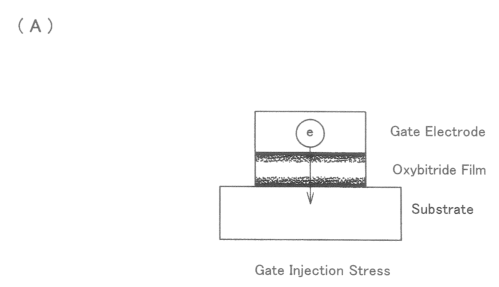
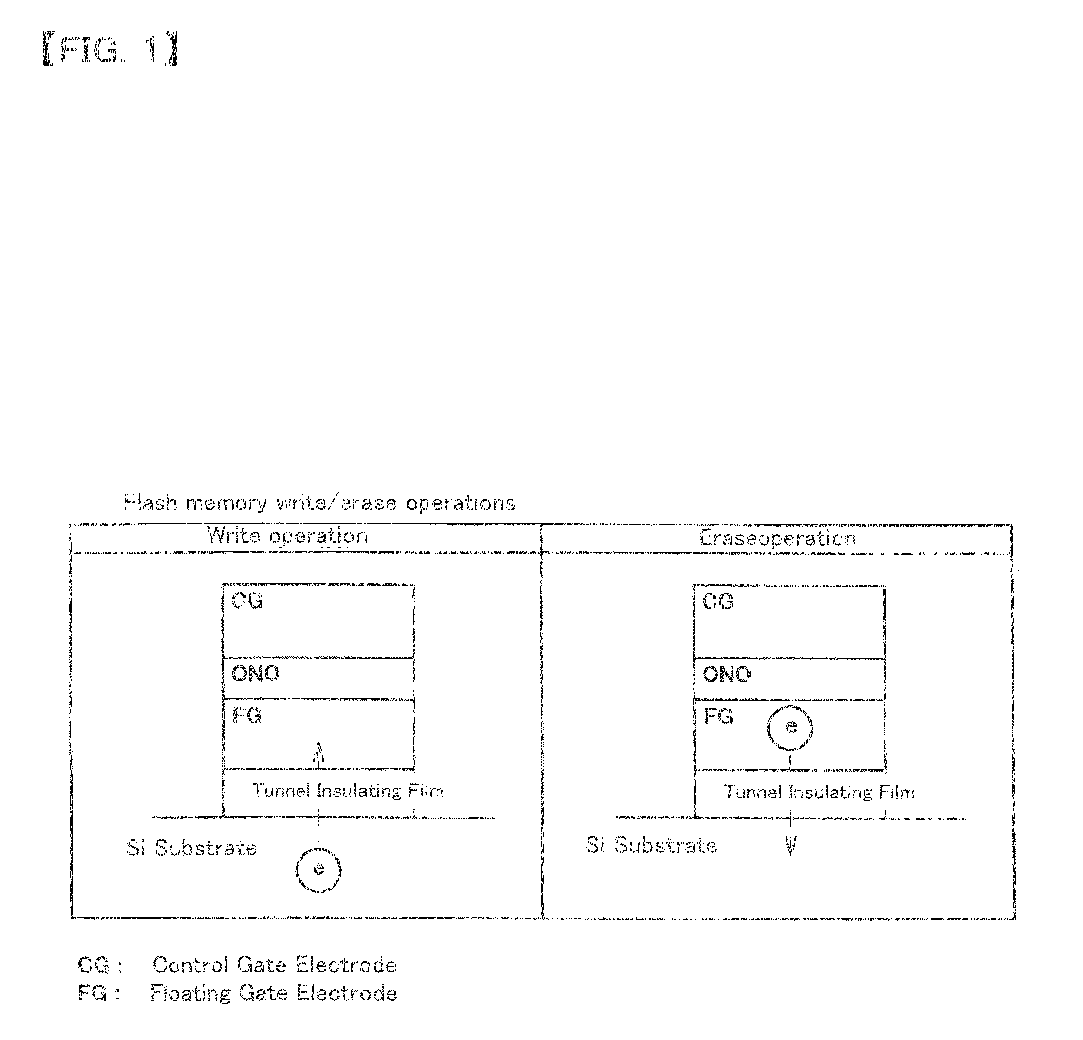
[0020]The present invention is applicable to a semiconductor storage device (flash memory, EEPROM or the like) which operates by transferring a charge through an insulating film.
[0021]FIG. 1 is an explanatory diagram showing examples of write and erase operations in flash memory, representing an application of the present invention. During a write operation, a charge flows from a silicon substrate to a gate electrode (FG: Floating Gate) through a tunnel insulating film. On the other hand, during an erase operation, a charge flows from the gate electrode (FG) to the silicon substrate through the tunnel insulating film. The present invention is characterized by the structure (nitrogen concentration profile) of the tunnel insulating film (gate insulating film).
[0022]To avoid damaging the gate insulating film, plasma processing of the film is performed using an RLSA (Radial Line Slot Antenna) microwave plasma processing apparatus, which produces a high density plasma with a low electron...
PUM
| Property | Measurement | Unit |
|---|---|---|
| Fraction | aaaaa | aaaaa |
| Flow rate | aaaaa | aaaaa |
| Percent by atom | aaaaa | aaaaa |
Abstract
Description
Claims
Application Information