Electronic board, method of manufacturing the same, and electronic device

Inactive Publication Date: 2006-12-21
138 EAST LCD ADVANCEMENTS LTD
View PDF10 Cites 6 Cited by
  • Summary
  • Abstract
  • Description
  • Claims
  • Application Information

AI Technical Summary

Benefits of technology

[0026] This constitution can provide an electronic

Problems solved by technology

Since techniques to form a capacitor on a semiconductor chip-mounting substrate entail the capacitor being disposed away from transistors on the semiconductor chip, it is difficult to ensure the response characteristics and high-frequency characteristics of the capacitor.
In addition, since a gate film is used as a dielectric layer in techniques to manufac

Method used


Image

  • Electronic board, method of manufacturing the same, and electronic device
  • Electronic board, method of manufacturing the same, and electronic device
  • Electronic board, method of manufacturing the same, and electronic device

Examples


first embodiment

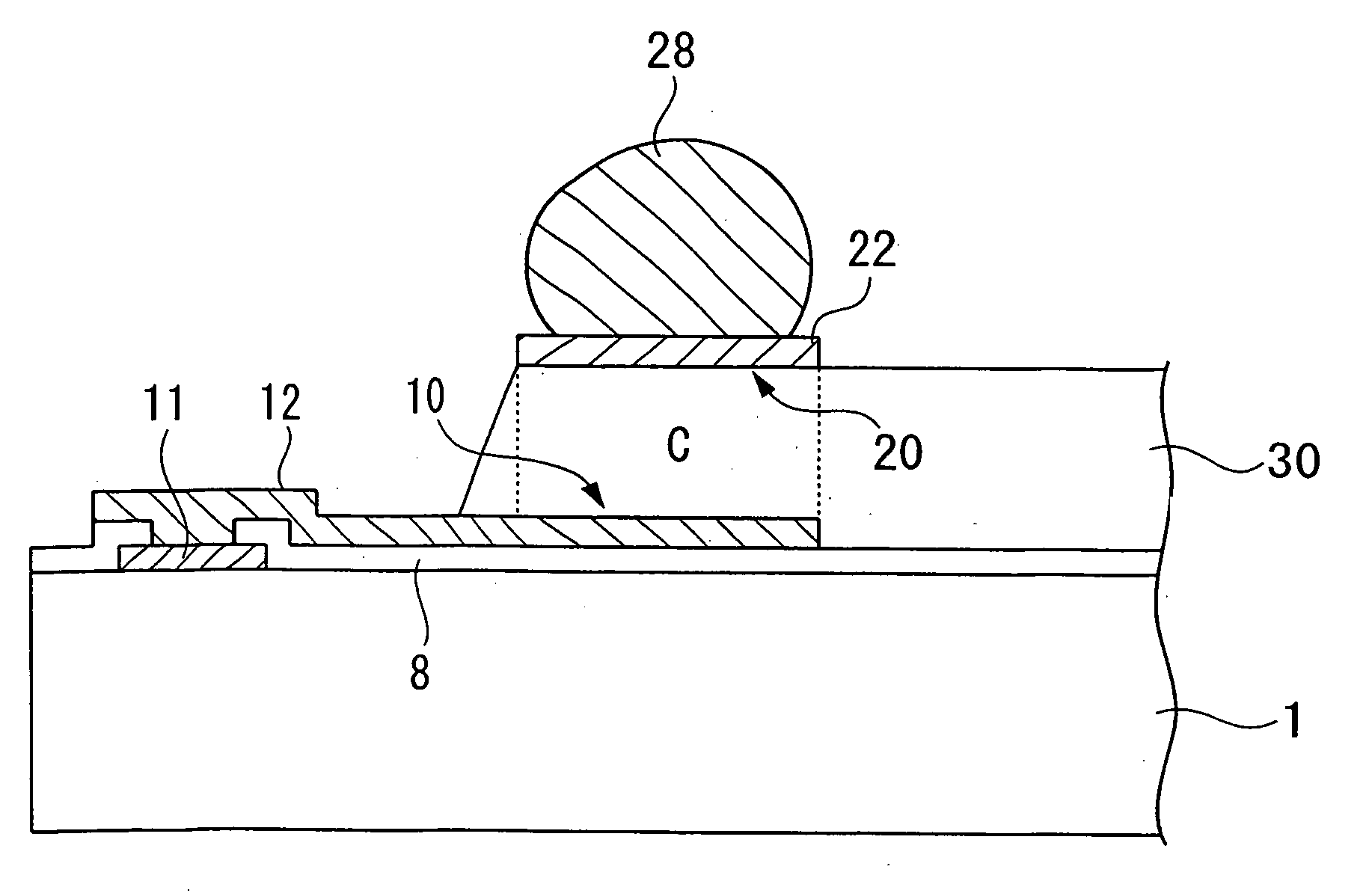
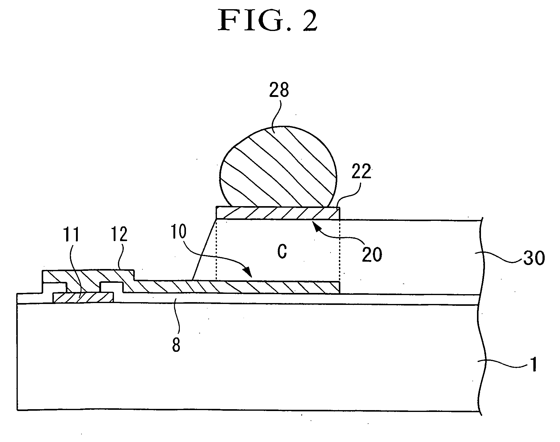
[0037] The semiconductor chip (electronic board) according to the present embodiment is one in which a stress-relaxation layer is formed on the surface of a semiconductor chip having an electronic circuit formed thereon, with rearrangement wiring for connection terminals of the electronic circuit formed on the surface of the stress-relaxation layer. The rearrangement wiring for the connection terminals and the stress-relaxation layer shall be initially explained.

[0038] Rearrangement Wiring

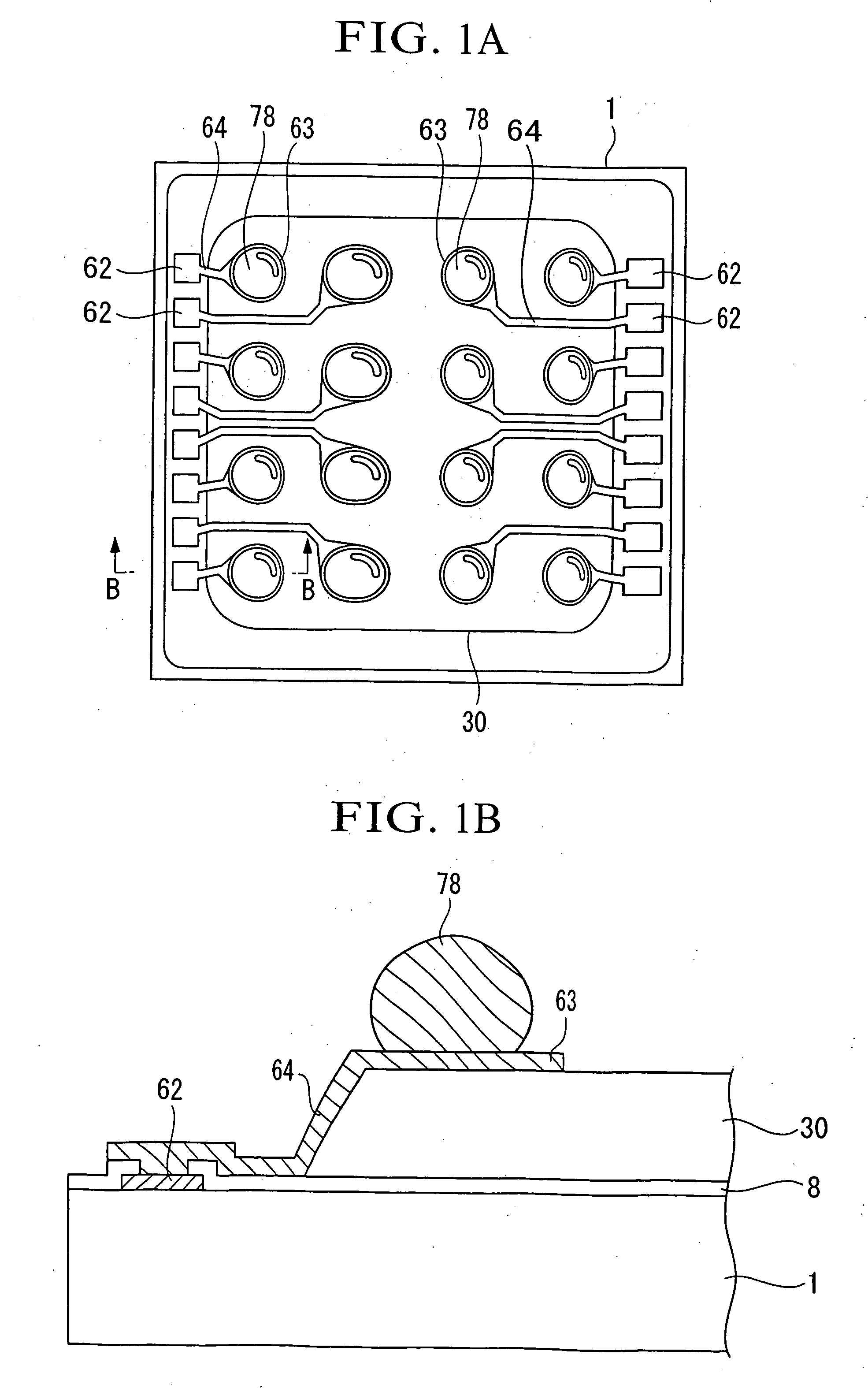
[0039]FIG. 1A and FIG. 1B are explanatory drawings of the rearrangement wiring, with FIG. 1A being a plan view of the semiconductor chip, and FIG. 1B being a side sectional view of the rearrangement wiring along line B-B in FIG. 1A. As shown in FIG. 1B, a passivation film 8 for protecting the electronic circuit is formed on the surface of the semiconductor chip on which the electronic circuit is formed. A connection terminal 62 for external electrical connection of the electronic circuit is forme...

second embodiment

[0067]FIG. 4A is a side-view sectional view of the semiconductor chip according to the second embodiment. In the second embodiment, the connection terminal 11 functions as the first electrode 10 of the capacitor C, thereby differing from the first embodiment in which the first layer wiring extended from the connection terminal functions as the first electrode. Detailed explanations for those constituent elements similar to the first embodiment shall be omitted.

[0068] In the second embodiment, the stress-relaxation layer 30 is formed so as to cover the connection terminal 11. For that reason, a portion of the stress-relaxation layer 30 is either extended to the edge part of the surface of the semiconductor chip 1, or the connection terminal 11 is formed in advance toward the center portion of the semiconductor chip 1. The second layer wiring 22 is formed on the surface of the stress-relaxation layer 30 in the similar manner as in the first embodiment.

[0069] The capacitor C is forme...

third embodiment

[0073]FIG. 5A is a side sectional view of the semiconductor chip according to the third embodiment. While in the first embodiment the capacitor C is formed by using a single stress-relaxation layer in the dielectric layer, the third embodiment differs on the point the capacitor C being formed by using a plurality of stress-relaxation layers in the dielectric layer. Detailed explanations for those constituent elements similar to the first embodiment shall be omitted.

[0074] In the third embodiment, a first stress-relaxation layer 31 is formed in the center portion of the surface of the semiconductor chip 1, and a second stress-relaxation layer 32 is formed on the surface of the first stress-relaxation layer 31. The first layer wiring 12 is formed at the back side of the first stress-relaxation layer 31, and the second layer wiring 22 is formed on the surface of the second stress-relaxation layer 32.

[0075] The capacitor C is formed in the region where in the plan view the first layer...


PUM


Abstract

An electronic board includes: a substrate on which is formed an electronic circuit having a connection terminal; a stress-relaxation layer formed on the substrate; rearrangement wiring for the connection terminal disposed at a top side of the stress-relaxation layer; and a capacitor that has a first electrode that is disposed between the substrate and the stress-relaxation layer, a second electrode that is disposed at the top side of the stress-relaxation layer, and a dielectric material that is disposed between the first electrode and the second electrode.

Description

CROSS-REFERENCE TO RELATED APPLICATION [0001] This application claims priority to Japanese Patent Application No. 2005-180400, filed Jun. 21, 2005, the contents of which are incorporated herein by reference. BACKGROUND [0002] 1. Technical Field [0003] The present invention relates to an electronic board, a method of manufacturing the electronic board, and an electronic device. [0004] 2. Related Art [0005] Electronic devices such as mobile telephones and personal computers have mounted therein a semiconductor chip (electronic board) whereon an electronic circuit is formed. Such a semiconductor chip is used with passive elements such as resistors, inductors and capacitors. Japanese Unexamined Patent Application, First Publication Nos. 2000-340955, 2000-353875, and 2001-156456 disclose techniques of forming a capacitor on a substrate on which a semiconductor chip is mounted. In addition, Japanese Unexamined Patent Application, First Publication No. H02-162820 discloses a technique of f...

Claims


Application Information

Patent Timeline
IPC IPC(8): H01L23/48H01L23/52
CPCH01L23/3114H01L23/3171H01L24/13H01L23/5223H01L23/525H01L24/10H01L2224/13099H01L2224/16H01L2924/01013H01L2924/01029H01L2924/01033H01L2924/01074H01L2924/01078H01L2924/19041H01L2924/19042H01L2924/19043H01L2924/30105H01L2924/3011H01L2924/01005H01L2924/01006H01L2924/014H01L2924/00H01L24/03H01L24/05H01L2224/023H01L2224/05001H01L2224/05022H01L2224/05124H01L2224/05548H01L2224/06131H01L2224/13H01L2924/00014H01L2224/05599H01L2924/0001H05K1/18
Inventor HASHIMOTO, NOBUAKI
Owner 138 EAST LCD ADVANCEMENTS LTD
Why Eureka
Try Eureka