Vertical semiconductor devices

Active Publication Date: 2020-06-18
SAMSUNG ELECTRONICS CO LTD
View PDF0 Cites 5 Cited by
  • Summary
  • Abstract
  • Description
  • Claims
  • Application Information

AI Technical Summary

Benefits of technology

[0010]According to an exemplary embodiment of the present inventive concept, a vertical semiconductor device includes an etch stop layer pattern. A dry etching process is performed to expose the etch stop layer pattern, and

Problems solved by technology

A dry etching process may be performed to form memory cells stacked in the vertical direc

Method used


Image

  • Vertical semiconductor devices
  • Vertical semiconductor devices
  • Vertical semiconductor devices

Examples


Embodiment Construction

[0024]Example embodiments will be more clearly understood from the following detailed description taken in conjunction with the accompanying drawings.

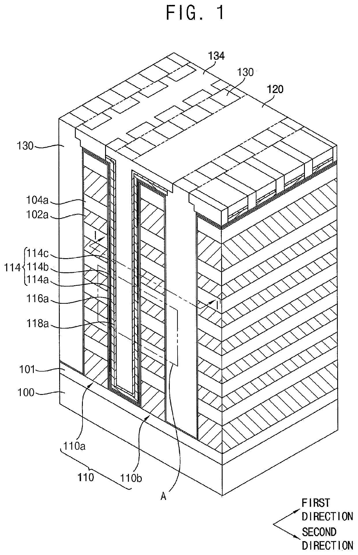
[0025]In the specification, a direction substantially parallel to an upper surface of a substrate is defined as a first direction. A direction substantially parallel to the upper surface of the substrate and perpendicular to the first direction is defined as a second direction. A direction substantially perpendicular to the upper surface of the substrate is defined as a vertical direction.

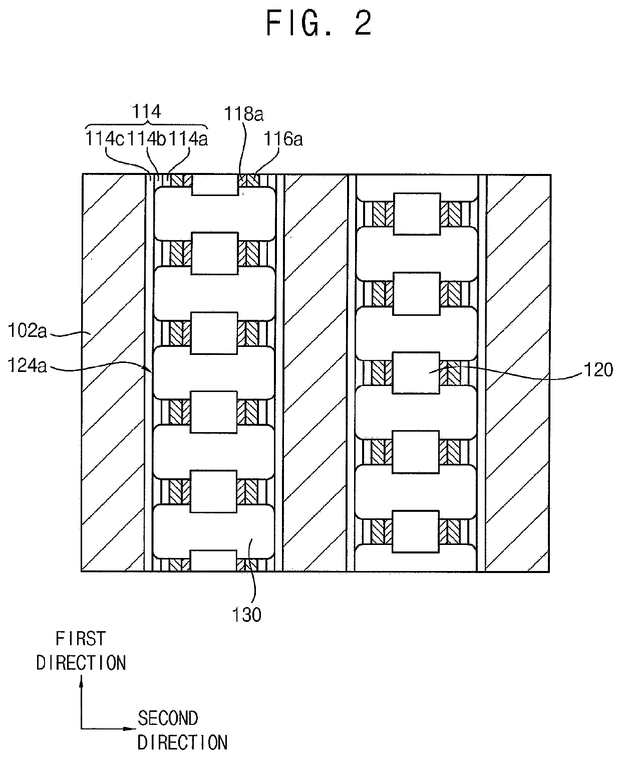
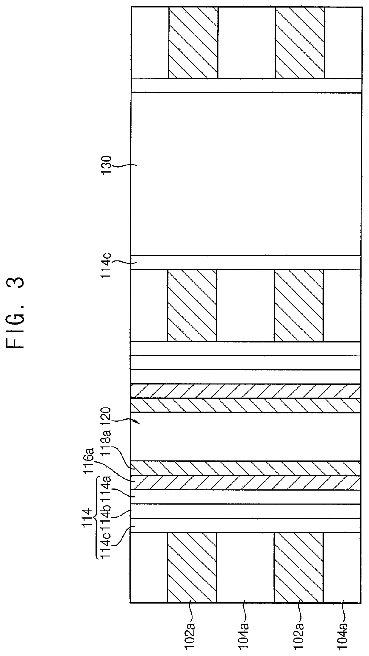
[0026]FIG. 1 is a perspective view illustrating a vertical semiconductor device in accordance with example embodiments. FIGS. 2 and 3 are a plan view and a cross-sectional view illustrating portions of vertical semiconductor devices in accordance with example embodiments, respectively. FIGS. 4 and 5 are a plan view and a cross-sectional view illustrating portions of a vertical semiconductor device in accordance with example embodiments.

[0027]Each of F...


PUM


Abstract

A vertical semiconductor device includes conductive pattern structures extending in a first direction, a trench between two adjacent conductive pattern structures in a second direction crossing the first direction, a memory layer disposed on sidewalls of the trench, first insulation layers disposed in the trench and spaced apart from each other in the first direction, channel patterns disposed on the memory layer and in the trench and spaced apart from each other in the first direction, and etch stop layer patterns disposed in the trench. Each conductive pattern structure includes conductive patterns and insulation layers alternately stacked on an upper surface of the substrate. Each etch stop layer pattern is disposed between a corresponding first insulation layer and the blocking dielectric layer. Etch stop layer patterns are spaced apart from each other in the first direction.

Description

CROSS-REFERENCE TO RELATED APPLICATION[0001]This application claims priority under 35 USC § 119 to Korean Patent Application No. 10-2018-0159713, filed on Dec. 12, 2018 in the Korean Intellectual Property Office (KIPO), the contents of which are incorporated by reference herein in their entirety.BACKGROUND1. Field[0002]Example embodiments relate to vertical semiconductor devices. More particularly, example embodiments relate to vertical semiconductor devices having a stable structure.2. Description of the Related Art[0003]Vertical semiconductor devices including a plurality of memory cells vertically stacked at a plurality of levels, respectively, on a substrate have been developed. A dry etching process may be performed to form memory cells stacked in the vertical direction, and thus, etching damages may occur at layer patterns included in the memory cells.SUMMARY[0004]Example embodiments provide a vertical semiconductor device vertical semiconductor device having improved electric...

Claims


Application Information

Patent Timeline
IPC IPC(8): H01L27/11582H01L27/11565H01L21/768H01L21/762H01L21/311
CPCH01L27/11582H01L21/31116H01L27/11565H01L21/76224H01L21/76832H01L21/76831H10B43/50H10B43/27H01L29/7926H10B43/10H01L29/732H01L29/4236H01L29/1025H01L21/76816H01L21/76829H01L21/30604H01L21/02532H01L21/02178H01L21/76837
Inventor LEE, KYUNG-HWANKIM, YONG-SEOKLIM, JUN-HEEKANAMORI, KOHJI
Owner SAMSUNG ELECTRONICS CO LTD
Why Eureka
Try Eureka