Organic electroluminescence device and electronic apparatus

an electroluminescence device and electronic equipment technology, applied in the direction of basic electric elements, electrical equipment, semiconductor devices, etc., can solve the problems of insufficient device performance of conventional organic el devices, and achieve the effect of large work function and high emitting property

Pending Publication Date: 2022-07-28
IDEMITSU KOSAN CO LTD
View PDF0 Cites 0 Cited by
  • Summary
  • Abstract
  • Description
  • Claims
  • Application Information

AI Technical Summary

Benefits of technology

[0611]Hereinafter, a device configuration, a material constituting each layer, and the like of the organic EL device according to an aspect of the invention will be described.
[0612]As a typical device configuration of the organic EL device, a configuration in which the following structure is stacked on a substrate is exemplified.
[0613]The electron-transporting zone is normally composed of one or more layers selected from an electron-injecting layer and an electron-transporting layer. Hereinafter, each layer of the organic EL device will be described.
[0614]A substrate is used as a support of an emitting device. As the substrate, glass, quartz, plastic or the like can be used, for example. Further, a flexible substrate may be used. The “flexible substrate” means a bendable (flexible) substrate, and specific examples thereof include a plastic substrate formed of polycarbonate, polyvinyl chloride, or the like.
[0615]For the anode formed on the substrate, metals, alloys, electrically conductive compounds, mixtures thereof, and the like, which have a large work function (specifically 4.0 eV or more) are preferably used. Specific examples include indium oxide-tin oxide (ITO: Indium Tin Oxide), indium oxide-tin oxide containing silicon or silicon oxide, indium oxide-zinc oxide, tungsten oxide, indium oxide containing zinc oxide, graphene, and the like. In addition thereto, specific examples thereof include gold (Au), platinum (Pt), a nitride of a metallic material (for example, titanium nitride), and the like.
[0616]The emitting layer is a layer containing a substance having a high emitting property, and various materials can be used for forming it. For example, as the substance having a high emitting property, a fluorescent compound which emits fluorescence or a phosphorescent compound which emits phosphorescence can be used. The fluorescent compound is a compound which can emit from a singlet excited state, and the phosphorescent compound is a compound which can emit from a triplet excited state.

Problems solved by technology

The device performance of the conventional organic EL device was still not sufficient.

Method used


Image

  • Organic electroluminescence device and electronic apparatus
  • Organic electroluminescence device and electronic apparatus
  • Organic electroluminescence device and electronic apparatus

Examples


example 1

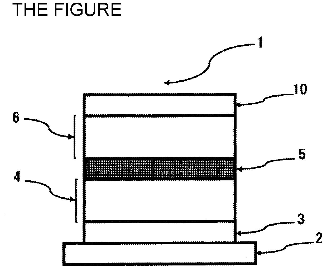
[0638]A 25 mm×75 mm×1.1 mm-thick glass substrate with an ITO transparent electrode (anode) (manufactured by GEOMATEC Co., Ltd.) was subjected to ultrasonic cleaning in isopropyl alcohol for 5 minutes, and then subjected to UV-ozone cleaning for 30 minutes. The thickness of the ITO film was 130 nm.

[0639]The glass substrate with the transparent electrode after being cleaned was mounted onto a substrate holder in a vacuum vapor deposition apparatus. First, Compound HA was deposited on a surface on the side on which the transparent electrode was formed so as to cover the transparent electrode to form a hole-injecting layer having a thickness of 1 nm.

[0640]On the hole-injecting layer, Compound HT was deposited to form a first hole-transporting layer having a film thickness of 80 nm.

[0641]On the first hole-transporting layer, Compound EBL-1 was deposited to form a second hole-transporting layer having a film thickness of 10 nm.

[0642]Compound BH (host material) and Compound BD (dopant mate...

example 2

[0662]An organic EL device was fabricated and evaluated in the same manner as in Example 1, except that Compound EBL-1 of Example 1 was replaced with EBL-2 in forming the first hole-transporting layer. The results are shown in Table 2.

example 3

[0666]An organic EL device was fabricated in the same manner as in Example 1, except that a hole-injecting layer having a film thickness of 3 nm was formed in forming the first hole-transporting layer.


PUM

PropertyMeasurementUnit
thicknessaaaaaaaaaa
ionization potentialaaaaaaaaaa
thicknessaaaaaaaaaa

Abstract

An organic electroluminescence device, comprising: a cathode, an anode, an emitting layer disposed between the cathode and the anode, and a hole-transporting zone disposed between the anode and the emitting layer, wherein the hole-transporting zone contains a first layer and a second layer in this order from the anode side, the first layer contains a compound represented by the following formula (1), and the first layer has a thickness of 0.10 to 3.00 nm.

Description

TECHNICAL FIELD[0001]Embodiments described herein generally relate to novel organic electroluminescence device and electronic apparatus.BACKGROUND ART[0002]When voltage is applied to an organic electroluminescence device (hereinafter, also referred to as an organic EL device), holes and electrons are injected into an emitting layer from an anode and a cathode, respectively. Then, thus injected holes and electrons are recombined in the emitting layer, and excitons are formed therein.[0003]The device performance of the conventional organic EL device was still not sufficient. Although the improvement of the material used for the organic EL device is progressing gradually in order to raise the device performance, further performance enhancement is required.[0004]In order to enhance the performance of a device, various layer configurations have been studied, and for example, Patent Documents 1 and 2 disclose organic EL devices containing a specific amine compound in a hole-transporting z...

Claims


Application Information

Patent Timeline
Patent Type & Authority Applications(United States)
IPC IPC(8): H01L51/00
CPCH01L51/0072H01L51/0061H01L51/0055H01L51/0073H01L51/5056H01L51/006H01L51/0058H01L51/0074H01L51/0056H01L51/0094H10K85/623H10K85/636H10K85/6574H10K85/6572H10K50/156H10K50/17H10K85/40H10K85/624H10K85/626H10K85/633H10K85/6576H10K50/15
Inventor YAMADA, KEITARONAKAMURA, MASATO
Owner IDEMITSU KOSAN CO LTD
Why Eureka
Try Eureka