Organic electroluminescence device and electronic apparatus using the same

Pending Publication Date: 2022-08-18
IDEMITSU KOSAN CO LTD
View PDF0 Cites 0 Cited by
  • Summary
  • Abstract
  • Description
  • Claims
  • Application Information

AI Technical Summary

Benefits of technology

The invention provides a method for making organic EL devices by using specific compounds in the emitting layer, electron-transporting layer, and hole-injecting layer. The device has a cathode, an anode, and an organic layer containing the first and second compounds. The substrate can be a flexible substrate made of plastic or glass. The anode is made of a metal, metal alloy, or electrically conductive compound. The hole-injecting layer is made of molybdenum oxide, titanium oxide, vanadium oxide, rhenium oxide, chromium oxide, zirconium oxide, hafnium oxide, tantalum oxide, silicon oxide, serotonin, or a polymer compound. The hole-transporting layer is made of an aromatic amine compound, a carbazole derivative, an anthracene derivative, or a polymer compound. The patent allows for the use of these specific compounds in the device, but other substances with similar properties can also be used. The invention also provides a method for making flexible organic EL devices using a flexible substrate.

Problems solved by technology

However, the organic EL devices disclosed in Patent Documents 1 to 4 do not have sufficient lifetime, and there is room for improvement.

Method used


Image

  • Organic electroluminescence device and electronic apparatus using the same
  • Organic electroluminescence device and electronic apparatus using the same
  • Organic electroluminescence device and electronic apparatus using the same

Examples


example 1

(Fabrication of Organic EL Device)

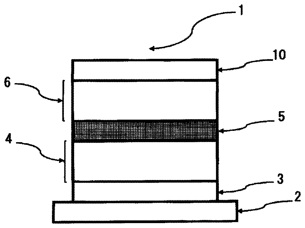
[0656]A 25 mm×75 mm×1.1 mm-thick glass substrate with an ITO transparent electrode (anode) (manufactured by GEOMATEC Co., Ltd.) was subjected to ultrasonic cleaning in isopropyl alcohol for 5 minutes, and then subjected to UV-ozone cleaning for 30 minutes. The thickness of the ITO film was 130 nm.

[0657]The glass substrate with the transparent electrode after being cleaned was mounted onto a substrate holder in a vacuum vapor deposition apparatus. First, a compound HI was deposited on a surface on the side on which the transparent electrode was formed so as to cover the transparent electrode to form an HI film having a thickness of 5 nm. This HI film functions as a hole-injecting layer.

[0658]A compound HT was deposited on the HI film to form an HT film having a thickness of 90 nm. This HT film functions as a hole-transporting layer (hereinafter, also referred to as an HT layer).

[0659]On this HT film, a compound BH (host material) and a compound BD-2 ...

example 37

[0673]The organic EL device was fabricated and evaluated in the same manner as in Example 1 except that the compounds shown in Table 3 were used as materials of the emitting layer, the first electron-transporting layer, and the second electron-transporting layer.

[0674]The second electron-transporting layer was formed by co-depositing a compound ET-2 and compound (8-quinolinolato)lithium (hereinafter, also referred to as Liq) so that the proportion of the compound Liq became 50% by mass to form an ET-2:Liq film having a thickness of 15 nm.

[0675]The layer structure of the obtained organic EL device is as follows. ITO(130) / HI(5) / HT(90) / BH:BD-1(25:4% by weight) / ET-A(10) / ET-2:Liq(15:50% by mass) / LiF(1) / Al(80)

[0676]Numerical values in parentheses indicate film thickness (unit: nm).

[0677]LT95 (unit: hours) of the obtained organic EL device was measured. Results are shown in Table 3.

example 42

(Fabrication of Organic EL Device)

[0681]A 25 mm×75 mm×1.1 mm-thick glass substrate with an ITO transparent electrode (anode) (manufactured by GEOMATEC Co., Ltd.) was subjected to ultrasonic cleaning in isopropyl alcohol for 5 minutes, and then subjected to UV-ozone cleaning for 30 minutes. The thickness of the ITO film was 130 nm.

[0682]The glass substrate with the transparent electrode after being cleaned was mounted onto a substrate holder in a vacuum vapor deposition apparatus. First, a compound HI was deposited on a surface on the side on which the transparent electrode was formed so as to cover the transparent electrode to form an HI film having a thickness of 5 nm. This HI film functions as a hole-injecting layer.

[0683]On this HI film, a compound HT was deposited to form an HT film having a thickness of 80 nm. This HT film functions as a hole-transporting layer (hereinafter, also referred to as an HT layer).

[0684]On this HT film, a compound HT-1 was deposited to form an HT-1 fi...


PUM


Abstract

An organic electroluminescence device comprising: a cathode, an anode, and an organic layer disposed between the cathode and the anode, wherein the organic layer comprises an emitting layer and an electron-transporting layer, the electron-transporting layer is disposed between the cathode and the emitting layer, the emitting layer comprises a first compound represented by any one of the formulas (21), (41), and (51), and the electron-transporting layer comprises a second compound represented by the following formula (B1):

Description

TECHNICAL FIELD[0001]The invention relates to an organic electroluminescence device and an electronic apparatus using the same.BACKGROUND ART[0002]When voltage is applied to an organic electroluminescence device (hereinafter, referred to as an organic EL device in several cases), holes and electrons are injected into an emitting layer from an anode and a cathode, respectively. Then, thus injected holes and electrons are recombined in the emitting layer, and excitons are formed therein.[0003]Patent Documents 1 to 4 disclose that compounds having a specific fused ring structure are used as a material for an emitting layer of an organic EL device.RELATED ART DOCUMENTSPatent Documents[0004][Patent Document 1] WO 2015 / 102118 A1[0005][Patent Document 2] WO 2016 / 152544 A1[0006][Patent Document 3] WO 2017 / 126443 A1[0007][Patent Document 4] WO 2017 / 188111 A1SUMMARY OF THE INVENTION[0008]However, the organic EL devices disclosed in Patent Documents 1 to 4 do not have sufficient lifetime, and ...

Claims


Application Information

Patent Timeline
IPC IPC(8): H01L51/00
CPCH01L51/0073H01L51/0055H01L51/0061H01L51/006H01L51/0058H01L51/0072H01L51/5012H01L51/0067H01L51/0052H01L51/0074H01L51/0054H01L51/0071H01L51/0059H01L51/008C09K11/06H10K85/623H10K85/622H10K85/626H10K85/615H10K85/654H10K85/6576H10K85/6574H10K85/6572H10K85/657H10K50/166H10K50/165H10K50/11H10K85/658H10K85/322H10K85/631H10K85/633H10K85/636H10K50/15H10K85/624H10K2101/10H10K2101/30
Inventor SAITO, MASATOSHIHAKETA, TASUKUNAKANO, YUKITASAKI, SATOMINISHIMURA, KAZUKI
Owner IDEMITSU KOSAN CO LTD
Why Eureka
Try Eureka