Organic electroluminescence device and electronic apparatus using the same
Pending Publication Date: 2022-03-03
IDEMITSU KOSAN CO LTD
View PDF0 Cites 1 Cited by
Summary
Abstract
Description
Claims
Application Information
AI Technical Summary
This helps you quickly interpret patents by identifying the three key elements:
Problems solved by technology
Method used
Benefits of technology
Benefits of technology
The invention relates to an organic EL device which includes a cathode, an anode, and an organic layer between them. The organic layer contains an emitting layer and an electron barrier layer. The invention is not impaired by the use of certain compounds in the device. The patent describes the materials that can be used to form the various layers of the device, including the substrate, anode, hole-injecting layer, hole-transporting layer, and guest material for emitting layer. The substrate can be made of glass or plastic, and the anode can be made of different metals or conductive compounds. The hole-injecting and hole-transporting layers can be made of various substances such as molybdenumoxide, titaniumoxide, or aromatic amine compounds, and can be present in a single layer or multiple layers. The use of certain compounds in the device is not impaired. The technical effects of the invention are improved performance and efficiency of organic EL devices.
Problems solved by technology
However, the organic EL devices disclosed in Patent Documents 1 to 8 are not sufficiently high in luminous efficiency, and there is room for improvement.
Method used
Image
Click on the blue label to locate the original text in one second.
Reading with bidirectional positioning of images and text.
Examples
example 1
(Fabrication of Organic EL Device)
[0783]A 25 mm×75 mm×1.1 mm-thick glass substrate with an ITO transparent electrode (anode) (manufactured by GEOMATEC Co., Ltd.) was subjected to ultrasonic cleaning in isopropylalcohol for 5 minutes, and then subjected to UV-ozone cleaning for 30 minutes. The thickness of the ITO film was 130 nm.
[0784]The glass substrate with the transparent electrode after being cleaned was mounted onto a substrate holder in a vacuum vapor deposition apparatus. First, a compound HI was deposited on a surface on the side on which the transparent electrode was formed so as to cover the transparent electrode to form an HI film having a thickness of 5 nm. This HI film functions as a hole-injecting layer.
[0785]On this HI film, a compound HT was deposited to form an HT film having a thickness of 80 nm. This HT film functions as a hole-transporting layer (hereinafter, also referred to as an HT layer).
[0786]On this HT film, a compound HT-1 was deposited to form an HT-1 fi...
example 30
(Fabrication of Organic EL Device)
[0799]A 25 mm×75 mm×1.1 mm-thick glass substrate with an ITO transparent electrode (anode) (manufactured by GEOMATEC Co., Ltd.) was subjected to ultrasonic cleaning in isopropylalcohol for 5 minutes, and then subjected to UV-ozone cleaning for 30 minutes. The thickness of the ITO film was 130 nm.
[0800]The glass substrate with the transparent electrode after being cleaned was mounted onto a substrate holder in a vacuum vapor deposition apparatus. First, a compound HI was deposited on a surface on the side on which the transparent electrode was formed so as to cover the transparent electrode to form an HI film having a thickness of 5 nm. This HI film functions as a hole-injecting layer.
[0801]On this HI film, a compound HT was deposited to form an HT film having a thickness of 80 nm. This HT film functions as a hole-transporting layer (hereinafter, also referred to as an HT layer).
[0802]On this HT film, a compound HT-1 was deposited to form an HT-1 fi...
examples 31 to 36
[0812]The organic EL devices were fabricated and evaluated in the same manner as in Example 30 except that compounds shown in Table 4 were used as materials of the EB layer and the first electron-transporting layer.
[0813]In Examples 31 to 36, the emitting layer was formed by co-depositing a compound BH (host material) and a compound BD-2 (dopant material) so that the proportion of the compound BD-2 became 4% by mass in the same manner as in Example 30.
[0814]In Example 34, the first electron-transporting layer was formed by co-depositing a compound ET-14 and a compound ET-13 so that the proportion of the compound ET-13 became 50% by mass.
PUM
Abstract
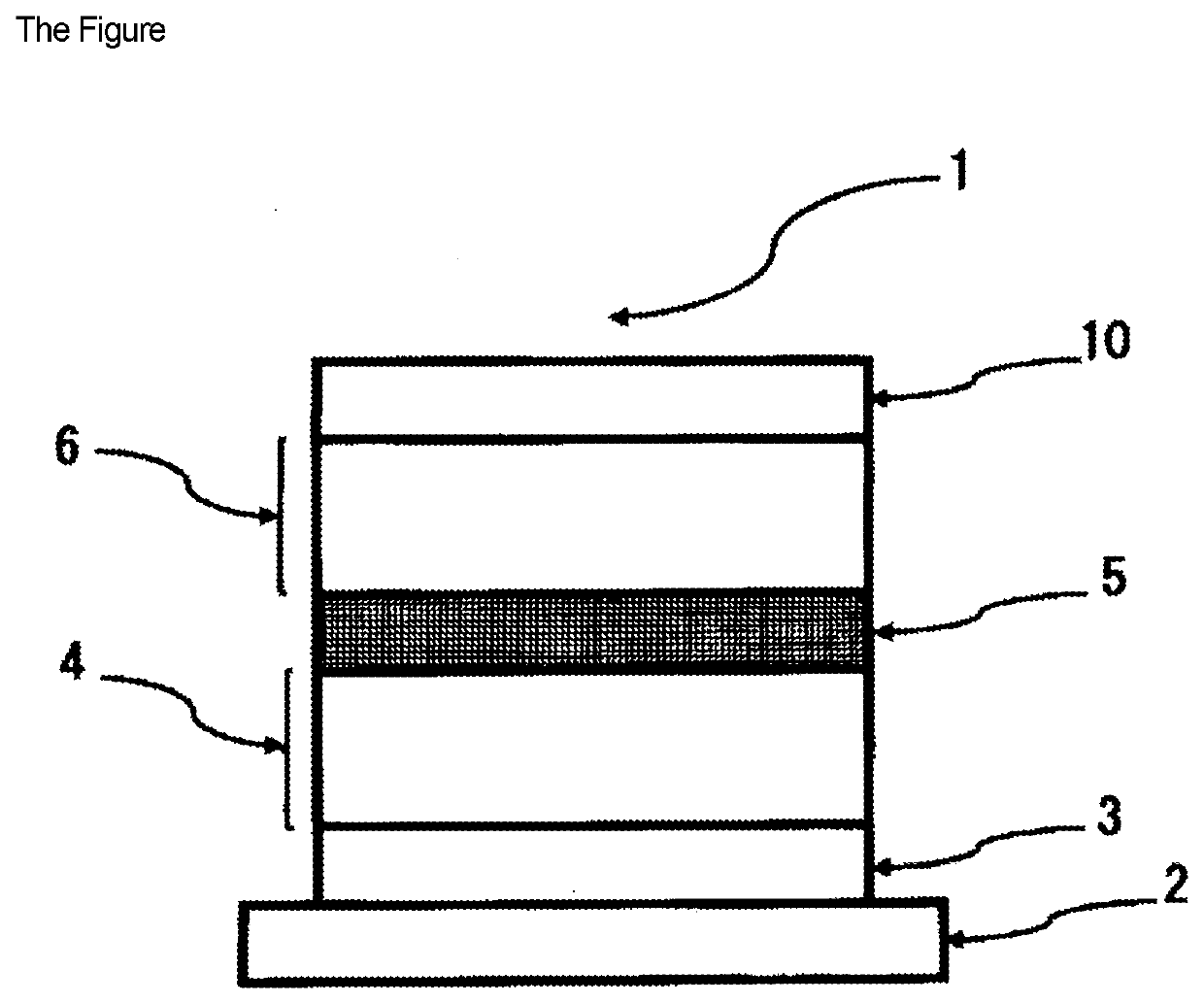
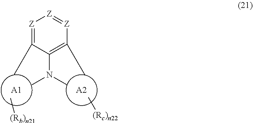
An organic electroluminescence device comprising:a cathode,an anode, andan organic layer disposed between the cathode and the anode,wherein the organic layer comprises an emitting layer and an electronbarrier layer,the electronbarrier layer is disposed between the anode and the emitting layer and is directly adjacent to the emitting layer,the emitting layer comprises a first compound represented by any one of the specific formulas (21), (41), and (51), andthe electronbarrier layer comprises a second compound which satisfies the following expression (M1):Ip(HT)≥5.67 eV (M1)wherein in the expression (M1), Ip(HT) is the ionization potential of the second compound.
Description
TECHNICAL FIELD[0001]The invention relates to an organic electroluminescence device and an electronic apparatus using the same.BACKGROUND ART[0002]When voltage is applied to an organic electroluminescence device (hereinafter, referred to as an organic EL device in several cases), holes and electrons are injected into an emitting layer from an anode and a cathode, respectively. Then, thus injected holes and electrons are recombined in the emitting layer, and excitons are formed therein.[0003]Patent Documents 1 to 4 disclose that compounds having a specific fused ring structure are used as a material for an emitting layer of an organic EL device.RELATED ART DOCUMENTSPatent Documents[0004][Patent Document 1] WD 2015 / 102118 A1[0005][Patent Document 2] W 2016 / 152544 A1[0006][Patent Document 3] W 2017 / 126443 A1[0007][Patent Document 4] W 2017 / 188111 A1SUMMARY OF THE INVENTION[0008]However, the organic EL devices disclosed in Patent Documents 1 to 8 are not sufficiently high in luminous ef...
Claims
Application Information
Patent Timeline
Application Date:The date an application was filed.
Publication Date:The date a patent or application was officially published.
First Publication Date:The earliest publication date of a patent with the same application number.
Issue Date:Publication date of the patent grant document.
PCT Entry Date:The Entry date of PCT National Phase.
Estimated Expiry Date:The statutory expiry date of a patent right according to the Patent Law, and it is the longest term of protection that the patent right can achieve without the termination of the patent right due to other reasons(Term extension factor has been taken into account ).
Invalid Date:Actual expiry date is based on effective date or publication date of legal transaction data of invalid patent.

