Semiconductor device
a technology of semiconductor devices and semiconductors, applied in semiconductor devices, semiconductor/solid-state device details, electrical apparatus, etc., can solve the problems of reducing the size of the wirings electrically connected to the transistors, and difficulty in high-speed operation, and achieve the effect of improving electrical characteristics
- Summary
- Abstract
- Description
- Claims
- Application Information
AI Technical Summary
Benefits of technology
Problems solved by technology
Method used
Image

Examples
Embodiment Construction
[0016]Hereinafter, example embodiments of the present inventive concept will be described with reference to the accompanying drawings.
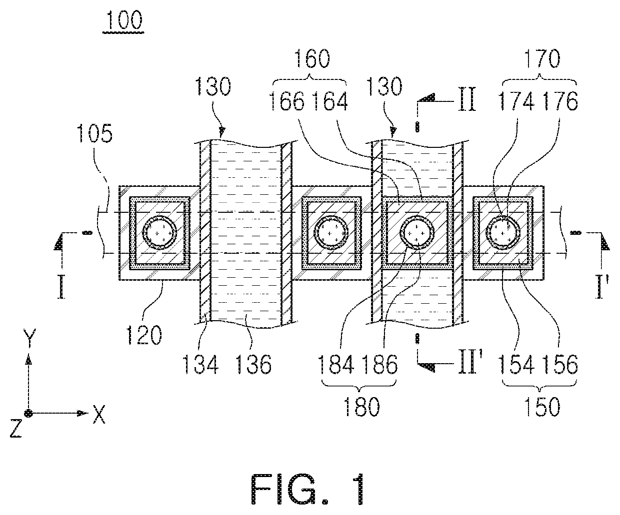
[0017]FIG. 1 is a plan view illustrating a semiconductor device according to an example embodiment of the present inventive concept.
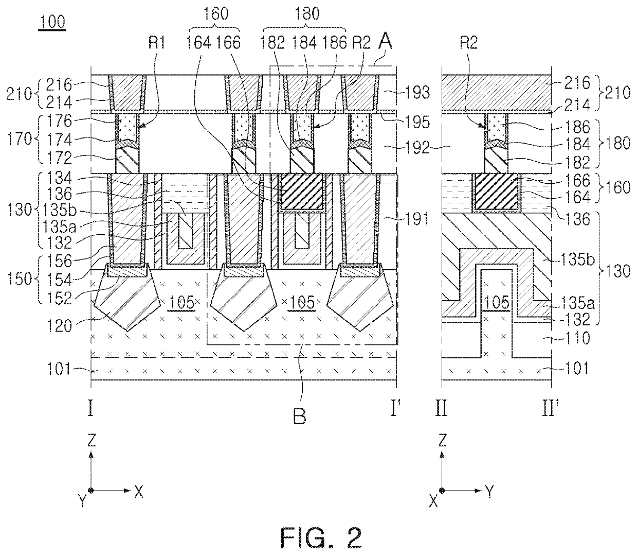
[0018]FIG. 2 is a cross-sectional view illustrating a semiconductor device according to an example embodiment of the present inventive concept. FIG. 2 is cross-sectional views of the semiconductor device of FIG. 1 taken along lines I-I′ and II-II′. For convenience of description, only major components of a semiconductor device are illustrated in FIGS. 1 and 2.
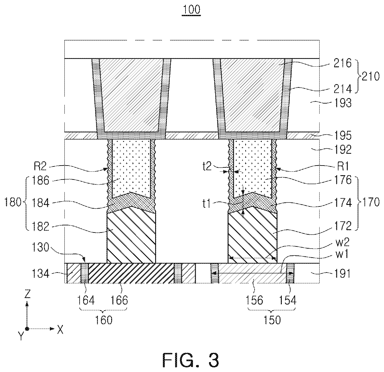
[0019]FIG. 3 is a partially enlarged cross-sectional view illustrating a semiconductor device according to an example embodiment of the present inventive concept. FIG. 3 is an enlarged view of region “A” of the semiconductor device of FIG. 1.
[0020]Referring to FIGS. 1 through 3, a semiconductor device 100 may include a substrate 101, an active region 105 on the subst...
PUM
| Property | Measurement | Unit |
|---|---|---|
| surface roughness | aaaaa | aaaaa |
| thickness | aaaaa | aaaaa |
| width | aaaaa | aaaaa |
Abstract
Description
Claims
Application Information