Display device using semiconductor light-emitting elements, and method for manufacturing same

Pending Publication Date: 2022-08-04
LG ELECTRONICS INC
View PDF0 Cites 0 Cited by
  • Summary
  • Abstract
  • Description
  • Claims
  • Application Information

AI Technical Summary

Benefits of technology

The present invention allows for a semiconductor light emitting device to be easily fixed onto a substrate using a photosensitive organic insulator. This process does not require applying pressure to the device or substrate, which prevents damage or deformation.

Problems solved by technology

However, in the case of LCD, there are problems in that the response time is not fast and flexible implementation is difficult, and in the case of AMOLED, there are weaknesses in that the lifespan is short and the mass production yield is not good.
On the other hand, in the case of a display using a semiconductor light emitting device, since the semiconductor light emitting device corresponding to each pixel must be coupled to the substrate, it may be relatively difficult to implement a large-screen high-pixel display.

Method used


Image

  • Display device using semiconductor light-emitting elements, and method for manufacturing same
  • Display device using semiconductor light-emitting elements, and method for manufacturing same
  • Display device using semiconductor light-emitting elements, and method for manufacturing same

Examples


Embodiment Construction

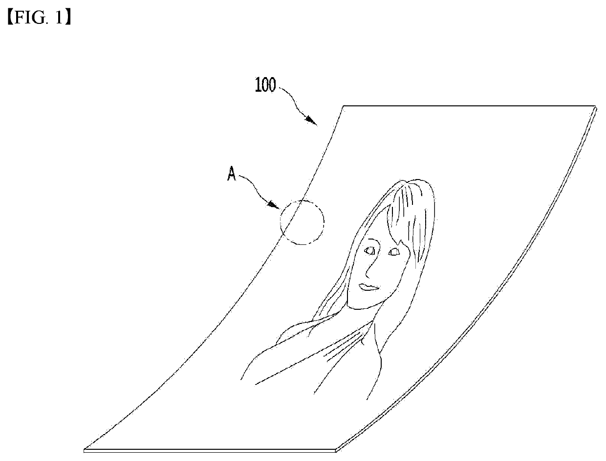
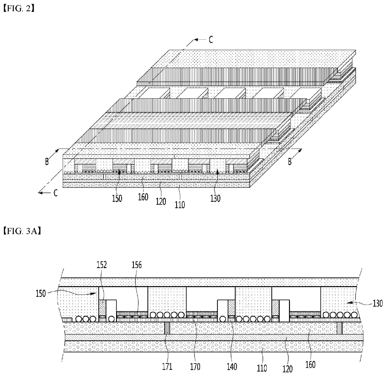
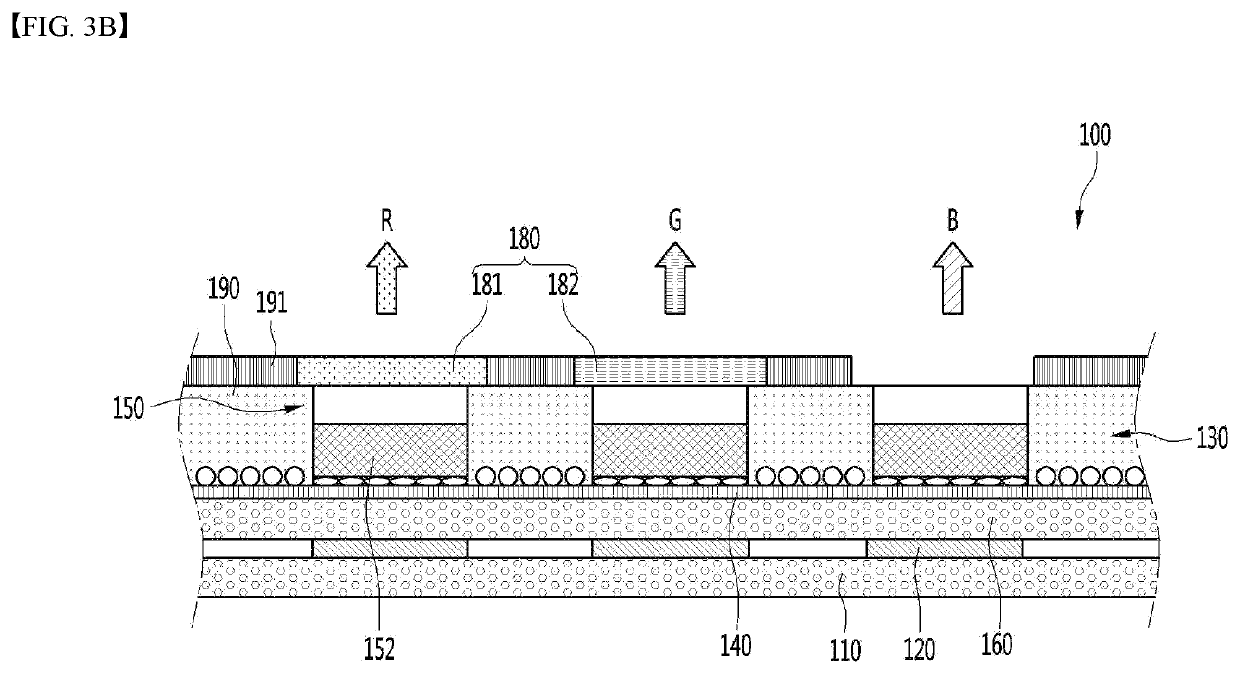
[0035]Hereinafter, the embodiments disclosed in the present specification will be described in detail with reference to the accompanying drawings, but the same or similar elements are given the same reference numbers regardless of reference numerals, and redundant description thereof will be omitted. The suffixes “module” and “part” for elements used in the following description are given or mixed in consideration of only the ease of writing the specification, and do not have distinct meanings or roles by themselves. In addition, in describing the embodiments disclosed in the present specification, if it is determined that detailed descriptions of related known technologies may obscure the gist of the embodiments disclosed in the present specification, the detailed description thereof will be omitted. In addition, it should be noted that the accompanying drawings are only for easy understanding of the embodiments disclosed in the present specification, and should not be construed as...


PUM


Abstract

A method for manufacturing a display device according to an embodiment of the present invention has a step for assembling semiconductor light-emitting devices on a substrate; a step for applying a photosensitive organic insulator onto the semiconductor light-emitting devices and the substrate; a step for removing the photosensitive organic insulator from the regions other than a space between the substrate and bottoms of the semiconductor light-emitting devices; and a step for curing the photosensitive organic insulator filled in the space.

Description

TECHNICAL FIELD[0001]The present invention relates to a display device using a semiconductor light emitting device and a method for manufacturing the same.BACKGROUND ART[0002]Recently, in the field of display technology, display devices having excellent characteristics such as thinness and flexibility have been developed. On the other hand, currently commercialized main displays are represented by LCD (Liquid Crystal Display) and AMOLED (Active Matrix Organic Light Emitting Diodes).[0003]However, in the case of LCD, there are problems in that the response time is not fast and flexible implementation is difficult, and in the case of AMOLED, there are weaknesses in that the lifespan is short and the mass production yield is not good.[0004]Meanwhile, a light emitting diode (Light Emitting Diode: LED) is a well-known semiconductor light emitting device that converts electric current into light. Starting with the commercialization of a red LED using a GaAsP compound semiconductor in 1962...

Claims


Application Information

Patent Timeline
IPC IPC(8): H01L25/075H01L33/38H01L33/62H01L33/44
CPCH01L25/0753H01L33/44H01L33/62H01L33/382H01L2933/0066H01L2933/0016H01L33/504H01L27/156H01L27/1259H01L27/1237
Inventor PARK, CHANGSEOMOON, SEONGMINJEON, KISEONG
Owner LG ELECTRONICS INC
Why Eureka
Try Eureka