Substrate, printing apparatus, and manufacturing method
a technology of printing apparatus and substrate, which is applied in the direction of typewriters, digital storage, instruments, etc., can solve the problems of limited number of anti-fuse elements to simultaneously write, wasteful in the viewpoint of product use after shipment, etc., and achieve the effect of increasing the write power
- Summary
- Abstract
- Description
- Claims
- Application Information
AI Technical Summary
Benefits of technology
Problems solved by technology
Method used
Image

Examples
first embodiment
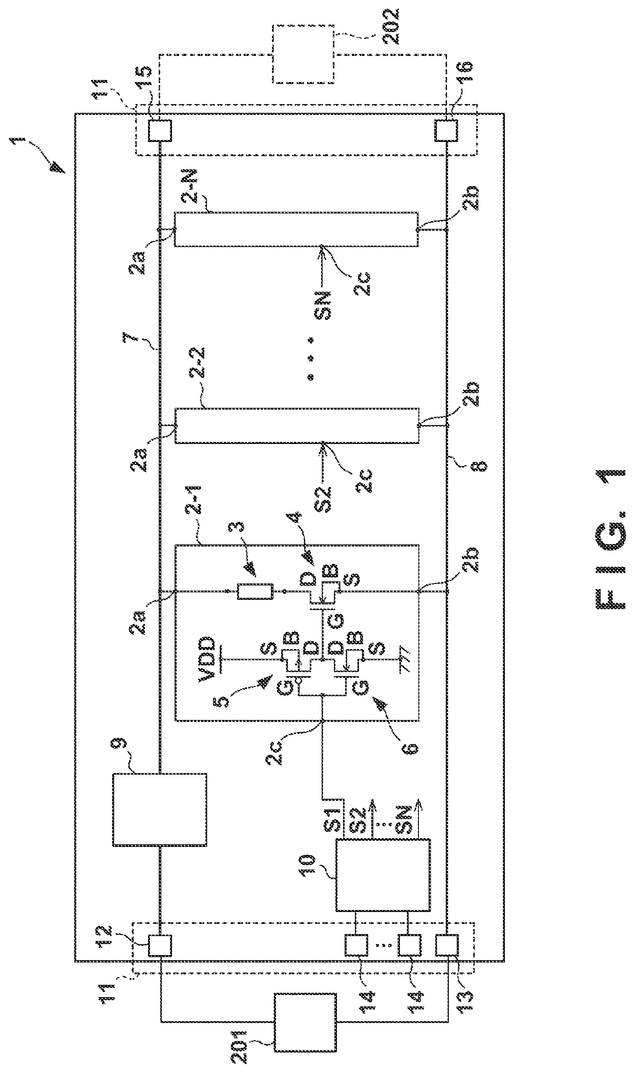
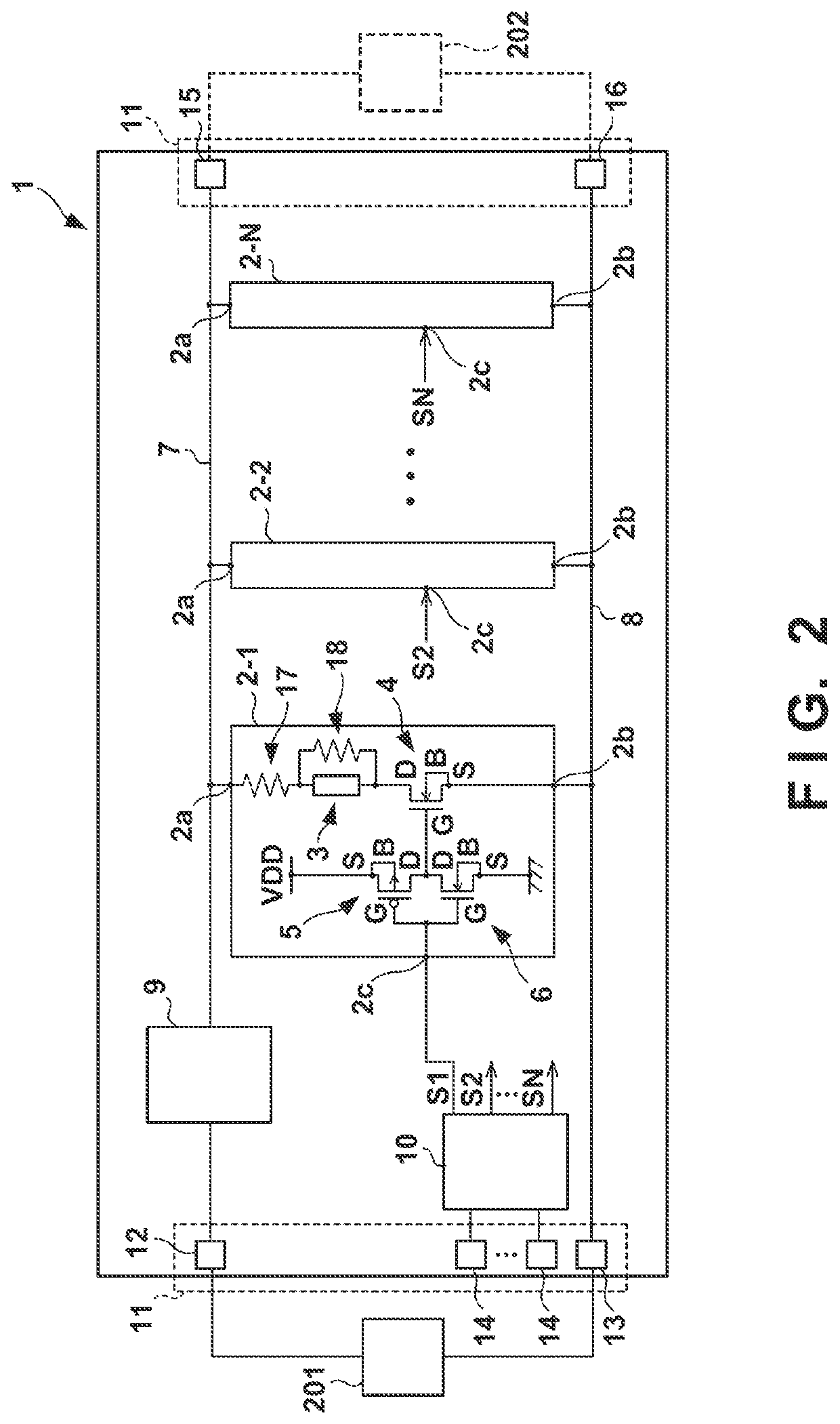
[0015]FIG. 1 is a circuit diagram of a substrate 1 according to an embodiment of the present invention. The substrate 1 is a storage device including a plurality of memory units 2-1 to 2-N. In this embodiment, N memory units 2-1 to 2-N are provided, which will be expressed as memory units 2 collectively or without distinction between individual memory units. Each memory unit 2 is a memory circuit including an anti-fuse element 3 and capable of holding 1-bit information. FIG. 1 shows the circuit of only the memory unit 2-1. The remaining memory units 2-2 to 2-N have the same circuit.
[0016]The anti-fuse element 3 is an element which has, for example, a MOS structure (Metal Oxide Semiconductor structure) and whose resistance value changes before and after information write. In this embodiment, the anti-fuse element 3 functions as a capacitance element before information is written, and functions as a resistive element after information is written. That is, the resistance value of the a...
second embodiment
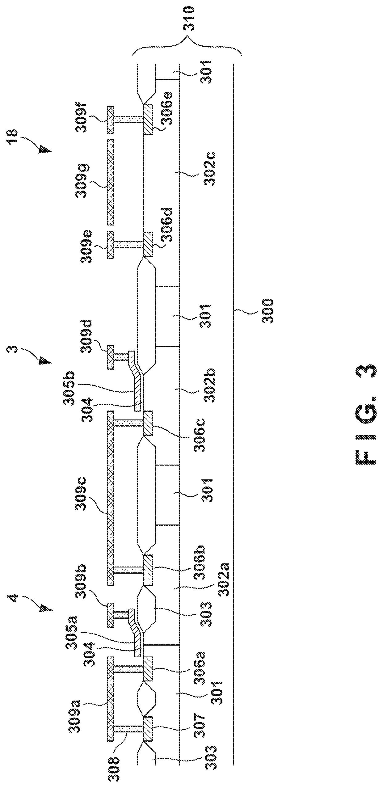
[0052]FIG. 4 is a view showing the outer appearance of a printing apparatus 30 according to an embodiment of the present invention. The printing apparatus 30 is an inkjet printing apparatus that performs printing on a print medium by discharging ink.
[0053]Note that “print” includes not only formation of significant information such as a character or graphic pattern but also formation of an image, design, or pattern on print media in a broader sense and processing of print media regardless of whether the information is significant or insignificant or has become obvious to allow human visual perception. Also, in this embodiment, “print medium” is assumed to be sheet-shaped paper but may be a fabric, a plastic film, or the like.
[0054]In addition, the printing apparatus to which the present invention can be applied is not limited to the inkjet printing apparatus, and the present invention can also be applied to, for example, a melt type or sublimation type thermal transfer printing appa...
PUM
| Property | Measurement | Unit |
|---|---|---|
| write voltage | aaaaa | aaaaa |
| drive voltage | aaaaa | aaaaa |
| voltage | aaaaa | aaaaa |
Abstract
Description
Claims
Application Information
 - R&D Engineer
- R&D Manager
- IP Professional
- Industry Leading Data Capabilities
- Powerful AI technology
- Patent DNA Extraction
Browse by: Latest US Patents, China's latest patents, Technical Efficacy Thesaurus, Application Domain, Technology Topic.
© 2024 PatSnap. All rights reserved.Legal|Privacy policy|Modern Slavery Act Transparency Statement|Sitemap