Micro light emitting diode display substrate and manufacturing method thereof

a technology of light-emitting diodes and display substrates, which is applied in the field of display technologies, can solve the problems of reducing display quality and high manufacturing cost (price/area), and achieve the effects of improving production rate, improving quality of spliced display, and simplifying structure and manufactur

Pending Publication Date: 2022-09-29
SHENZHEN CHINA STAR OPTOELECTRONICS SEMICON DISPLAY TECH CO LTD
View PDF6 Cites 0 Cited by
  • Summary
  • Abstract
  • Description
  • Claims
  • Application Information

AI Technical Summary

Benefits of technology

[0065]Compared to the prior art, the present invention manufactures a fanout circuit on the bottom surface of the underlay substrate, the fanout circuit can connect with a driver chip (IC) through bonding pads, and the bottom surface can further connect with an electro static protection circuit or the like. The TFT and Micro LED are manufactured on the top surface of the underlay substrate for display, the fanout circuit of the underlay substrate bottom surface and the display pixel (i.e., the TFT and the Micro LED) of the top surface of the underlay substrate are connected to the side printed bonding pad (side wiring pad) through the side wire aside the underlay substrate such that a display pixel region located on the top surface of the underlay substrate, after the micro light emitting diode display substrate is assembled with a bezel, can maximally approach the bezel to make a width of a splicing gap between the display pixel region and the bezel reach a size of one pixel unit and no obvious splicing mark at the macro level, which achieves a bezel-less effect. Therefore, using such technology on a spliced display has no obvious splicing non-displaying region among spliced displays, which improves the quality of the spliced display.
[0066]Furthermore, the present invention solution directly bonds the micro LED on the source and drain metal electrode layer of the TFT (i.e., the second source electrode / pixel electrode and the common cathode) without an independent process for forming holes in the passivation layer and an individual process for manufacturing the ITO pixel electrode layer. Only a common mask process is required for self-aligned patterning the passivation layer and the black matrix layer, which skips the additional processes for forming holes in the passivation layer and manufacturing the ITO pixel electrode layer. Therefore, the top surface of the display substrate only requires seven processes for completing manufacture of the TFT, which simplifies the structure and manufacture of the TFT surface of the display substrate and advantages improvement of the production rate and reduction of the manufacturing cost.

Problems solved by technology

In a field of displays such as liquid crystal display (LCD), organic light emitting diode (OLED), and light emitting diode (LED) displays, the greater a single screen body is, the higher a manufacturing cost (price / area) thereof is.
Because a display usually comprises a bezel, a displaying region of the spliced display has several strips of non-display dark regions, which lowers display quality.

Method used


Image

  • Micro light emitting diode display substrate and manufacturing method thereof
  • Micro light emitting diode display substrate and manufacturing method thereof
  • Micro light emitting diode display substrate and manufacturing method thereof

Examples


Embodiment Construction

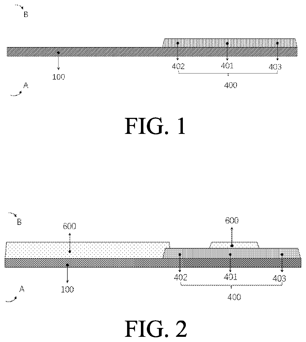
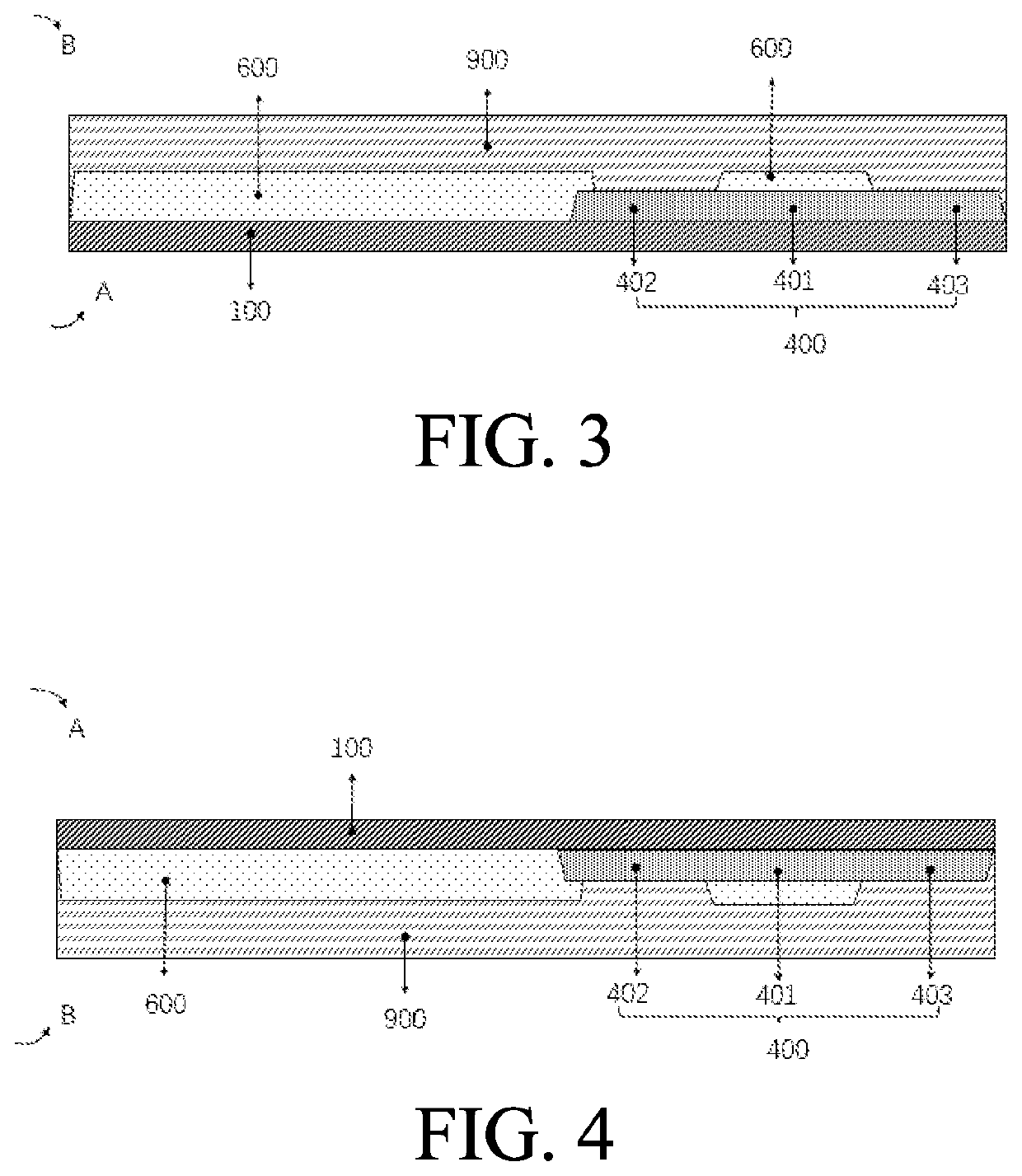
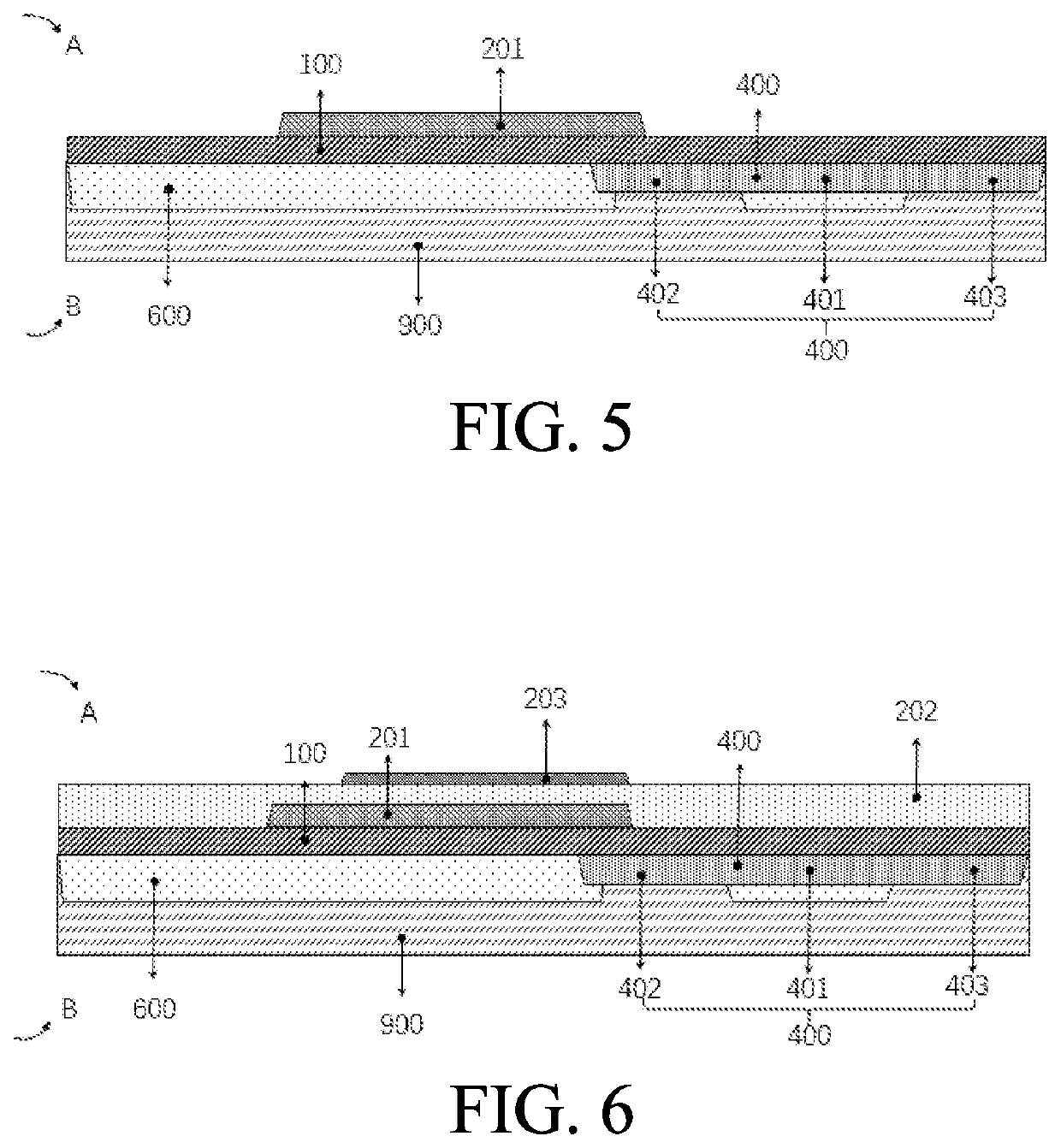
[0069]With reference to FIGS. 1 to 24, FIGS. 1 to 15 are schematic views of a manufacturing process of an embodiment of a micro light emitting diode display substrate of the present invention; FIGS. 16 to 24 are schematic views of a manufacturing process of another embodiment of the micro light emitting diode display substrate of the present invention. FIG. 15 is also a schematic structural view of the micro light emitting diode display substrate of an embodiment of the present invention. FIG. 24 is also a schematic structural view of the micro light emitting diode display substrate of another embodiment of the present invention. In the figures, A refers to a top surface of the underlay substrate 100, B refers to a bottom surface of the underlay substrate 100.

[0070]With reference to FIGS. 15 and 24, the embodiment of the present invention provides a micro light emitting diode display substrate, comprises an underlay substrate 100, a thin film transistor 200, a micro light emitting d...


PUM

PropertyMeasurementUnit
semiconductoraaaaaaaaaa
shieldingaaaaaaaaaa
sizeaaaaaaaaaa

Abstract

The present invention discloses a micro light emitting diode display substrate and a manufacturing method thereof. The substrate includes an underlay substrate, a thin film transistor and a micro light emitting diode disposed on a top surface of the underlay substrate and connected to each other, a first metal film layer disposed on a bottom surface of the underlay substrate and at least formed with fanout circuit pattern and a side printed bonding pad. The fanout circuit pattern is connected to the side printed bonding pad, the side printed bonding pad is connected to the thin film transistor through a side wire such that after the display substrate is assembled with a bezel, a top surface display pixel region can maximally approach the bezel, to achieve bezel-less effect.

Description

FIELD OF INVENTION[0001]The present invention relates to a field of display technologies, especially relates to a field of micro light emitting diode display device manufacturing technologies, specifically relates to a micro light emitting diode display substrate and a manufacturing method thereof.BACKGROUND OF INVENTION[0002]In a field of displays such as liquid crystal display (LCD), organic light emitting diode (OLED), and light emitting diode (LED) displays, the greater a single screen body is, the higher a manufacturing cost (price / area) thereof is. Therefore, a super large display usually is formed by splicing several small displays to lower the cost per area unit. Because a display usually comprises a bezel, a displaying region of the spliced display has several strips of non-display dark regions, which lowers display quality. Reducing a size of splicing gaps of a spliced display has become a popular research object in the industry.SUMMARY OF INVENTIONTechnical Issue[0003]The...

Claims


Application Information

Patent Timeline
Patent Type & Authority Applications(United States)
IPC IPC(8): H01L27/15H01L33/62
CPCH01L27/156H01L33/62H01L25/167H01L25/0753
Inventor LU, MACAIFAN, YONGLIU, MINGGANGLIU, NIANYAO, JIANGBO
Owner SHENZHEN CHINA STAR OPTOELECTRONICS SEMICON DISPLAY TECH CO LTD
Why Eureka
Try Eureka