Eureka AIR delivers breakthrough ideas for toughest innovation challenges, trusted by R&D personnel around the world.

Optical bridge interconnect unit for adjacent processors

Active Publication Date: 2022-10-06
ADVANCED MICRO DEVICES INC
View PDF2 Cites 0 Cited by
  • Summary
  • Abstract
  • Description
  • Claims
  • Application Information

AI Technical Summary

Benefits of technology

The patent text describes a computing system that efficiently transfers data between processing nodes using a communication bridge. The system includes a host processor and nodes that have processors and local memory. The nodes can be expansion cards or graphics cards that are inserted in sockets on a motherboard. The system also includes a communication fabric that allows for direct data transfer between processing nodes without the need for a system bus. The technical effect of the invention is to improve data transfer efficiency in a computing system, reducing bandwidth limitations and data corruption through data collision at the receiver.

Problems solved by technology

However, when connecting separate dies together via the interconnect, and when connecting separate processing nodes together, the data is transferred over a significantly lower number of physical wires, which limits available bandwidth.
However, there is still a significant bandwidth reduction when communicating between die and between nodes.
In addition, when a transmitter, such as a graphics processing unit (GPU) in a processing unit, sends packets at a rate faster than a rate that a receiver, such as the interconnect, can receive packets, data corruption occurs through data collision at the receiver.
A conservative approach of reducing the sending data rate of packets from the transmitter prevents data corruption, but it also further reduces the link bandwidth efficiency.

Method used


Image

  • Optical bridge interconnect unit for adjacent processors
  • Optical bridge interconnect unit for adjacent processors
  • Optical bridge interconnect unit for adjacent processors

Examples


Embodiment Construction

[0014]In the following description, numerous specific details are set forth to provide a thorough understanding of the present invention. However, one having ordinary skill in the art should recognize that the invention might be practiced without these specific details. In some instances, well-known circuits, structures, and techniques have not been shown in detail to avoid obscuring the present invention. Further, it will be appreciated that for simplicity and clarity of illustration, elements shown in the figures have not necessarily been drawn to scale. For example, the dimensions of some of the elements are exaggerated relative to other elements.

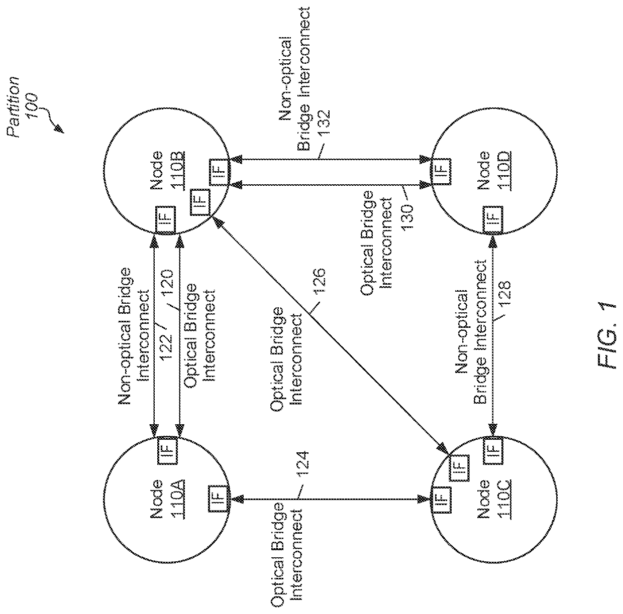
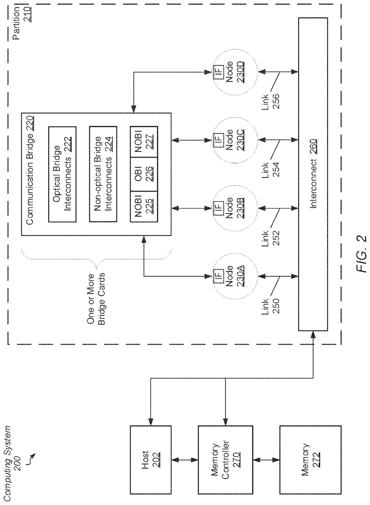
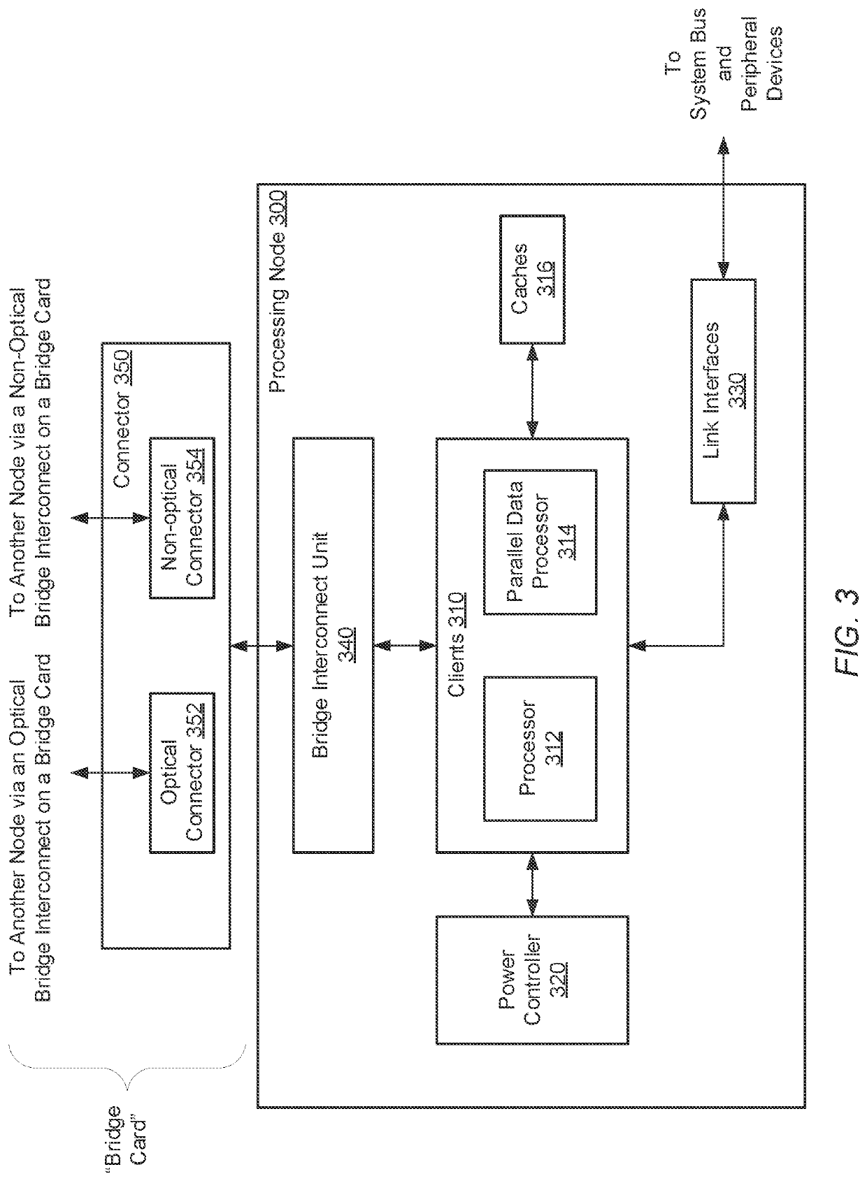
[0015]Various systems, apparatuses, and methods for performing efficient data transfer in a computing system are disclosed. In various embodiments, a computing system includes a host processor that assigns tasks to processing nodes of a multi-node partition. As used herein, a “processing node” is also referred to as a “node.” The nodes i...


PUM


Abstract

A system and method for efficient data transfer in a computing system are described. A computing system includes multiple nodes that receive tasks to process. A bridge interconnect transfers data between two processing nodes without the aid of a system bus on the motherboard. One of the multiple bridge interconnects of the computing system is an optical bridge interconnect that transmits optical information across the optical bridge interconnect between two nodes. The receiving node uses photonic integrated circuits to translate the optical information into electrical information for processing by electrical integrated circuits. One or more nodes switch between using an optical bridge interconnect and a non-optical bridge interconnect based on one or more factors such as measured power consumption and measured data transmission error rates.

Description

BACKGROUNDDescription of the Relevant Art[0001]In computing systems, multiple applications exploit parallel processing and large amounts of shared memory. Examples of these applications are machine learning applications, entertainment and real-time applications, as well as some business, scientific, medical and other applications. These computing systems use processing units (e.g., CPU, GPU, etc.) with more than one processing core, and, in some cases, use side-by-side stacked chips to offer more computational capability and / or more data storage. The processing units of these computing systems transmit and receive large amounts of data between one another and with a system memory. The data is transferred in this manner through an interconnect, such as a communication fabric, based on a particular communication protocol.[0002]In many cases, the interconnect transfers data while supporting relatively wide packets, since a high number of physical wires are available. However, when conn...

Claims


Application Information

Patent Timeline
IPC IPC(8): G06F13/40H04B10/80
CPCG06F13/4027H04B10/801G06F13/385H04Q11/00
Inventor RADKE, ROBERT E.JAGGERS, CHRISTOPHER M.
Owner ADVANCED MICRO DEVICES INC
Why Eureka
Eureka Blog
Learn More