

Apparatus for trapping multiple reaction by-products for semiconductor process
- Summary
- Abstract
- Description
- Claims
- Application Information
AI Technical Summary
Benefits of technology
Problems solved by technology
Method used
Image

Examples
Embodiment Construction
[0044]Hereinafter, configurations and operations of an exemplary embodiment of the present disclosure will be described in detail with reference to the accompanying drawings. In addition, in the description of the present disclosure, the specific descriptions of related well-known functions or configurations will be omitted when it is determined that the specific descriptions may unnecessarily obscure the subject matter of the present disclosure.
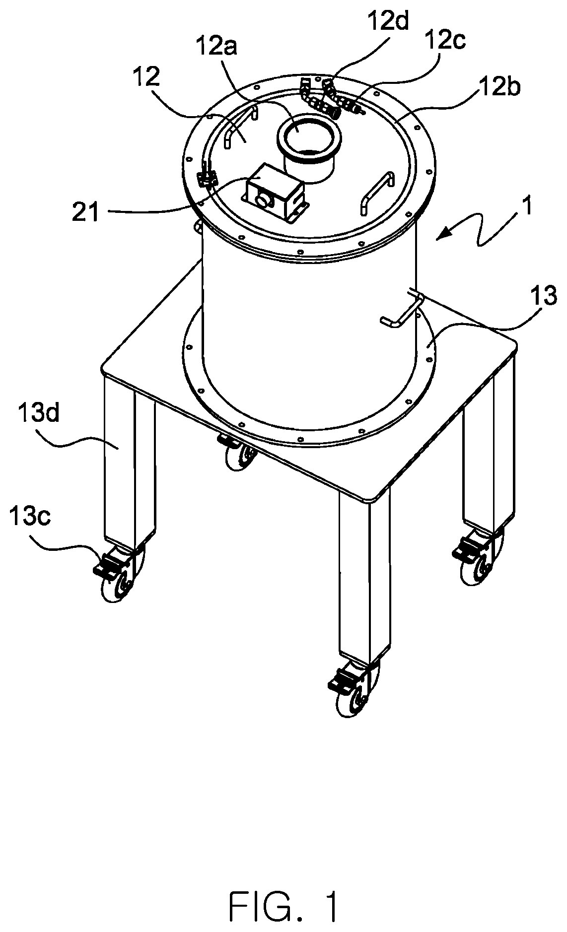
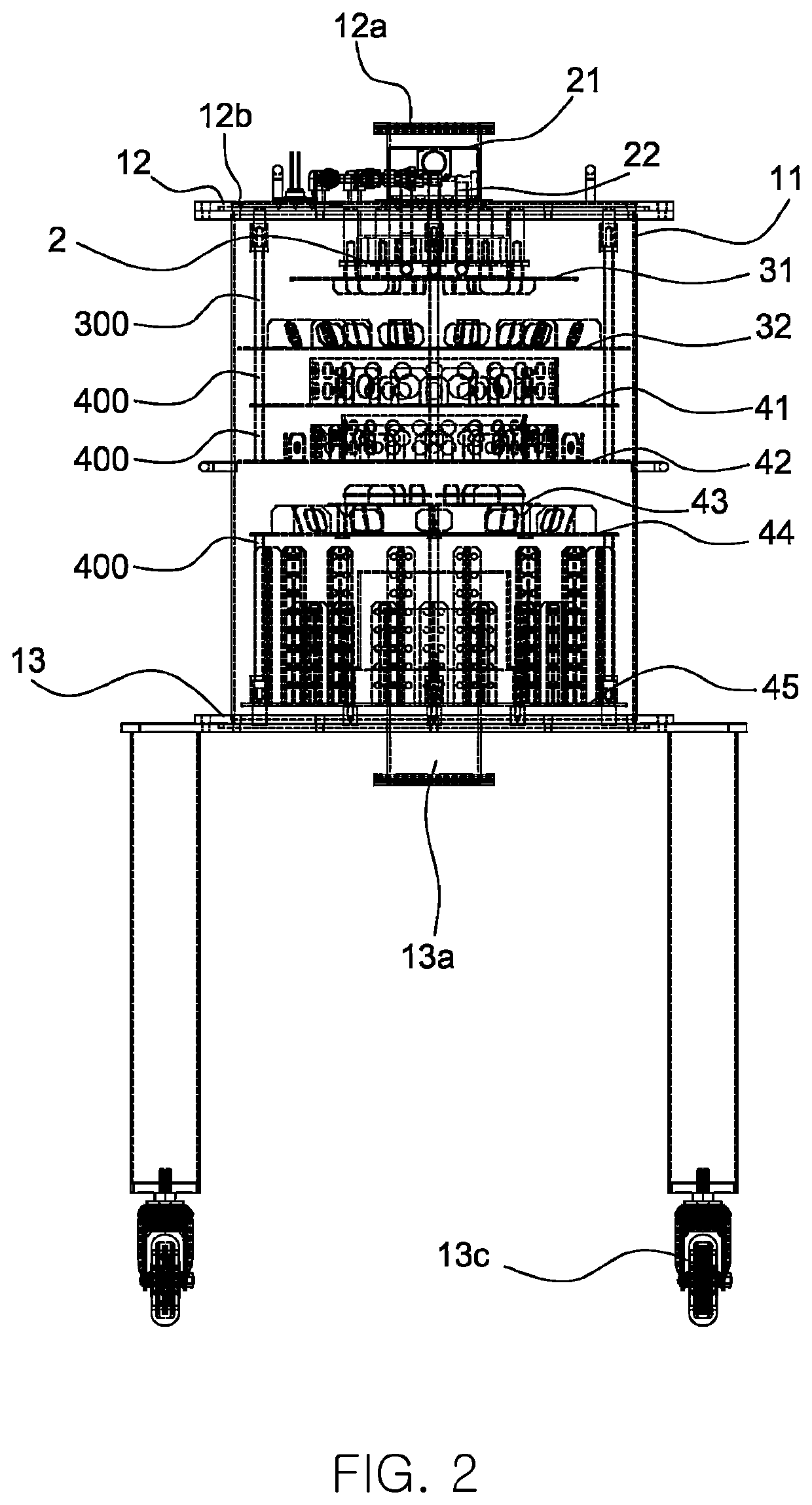
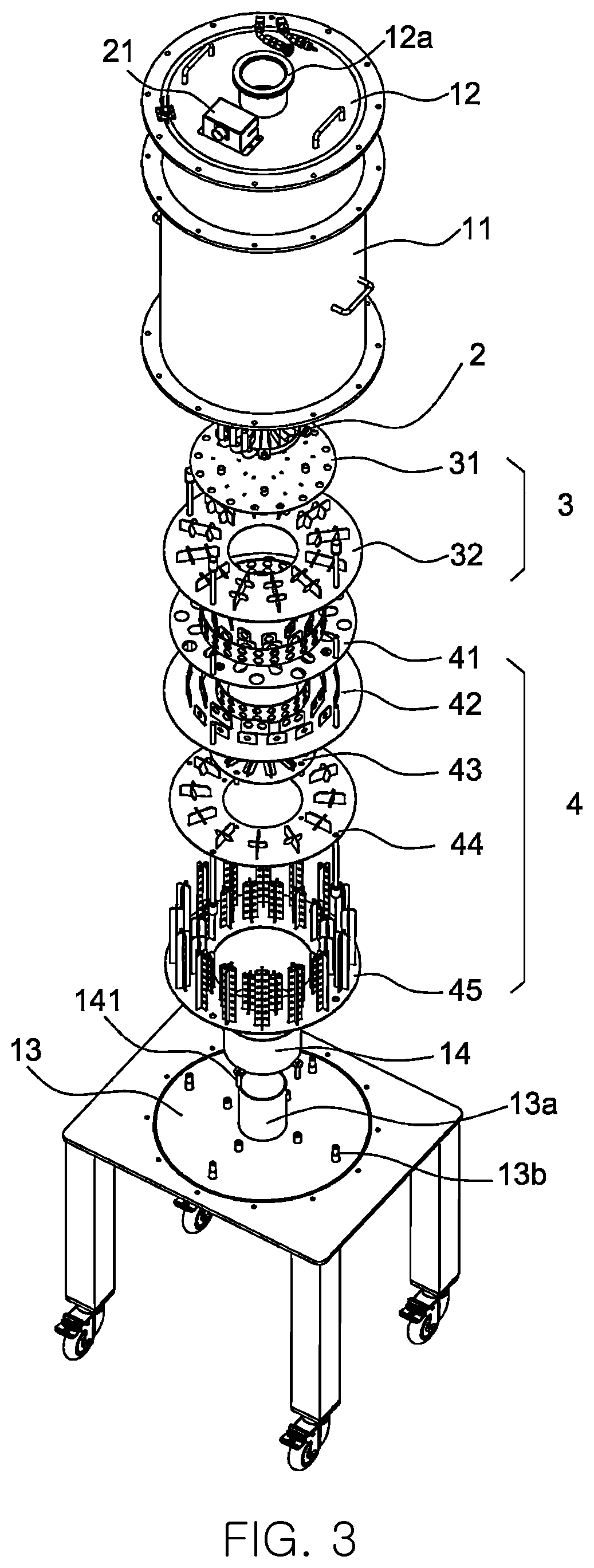
[0045]FIG. 1 is a perspective view illustrating a configuration of an apparatus for trapping multiple reaction by-products according to an embodiment of the present disclosure, FIG. 2 is a cross-sectional view illustrating an internal configuration of the apparatus for trapping multiple reaction by-products according to the embodiment of the present disclosure, and FIG. 3 is an exploded perspective view illustrating a configuration of the apparatus for trapping multiple reaction by-products according to the embodiment of the present disclosu...
PUM
 Abstract
Description
Claims
Application Information