Wafer surface treatment methods and systems using electrocapillarity

a surface treatment and electrocapillary technology, applied in the direction of photomechanical equipment, lapping machines, instruments, etc., can solve the problems of non-uniformity of the wafer surface, increased differences in the removal rate, and insufficient slurry transport to the center of the wafer

Inactive Publication Date: 2000-01-04
MICRON TECH INC
View PDF6 Cites 91 Cited by
  • Summary
  • Abstract
  • Description
  • Claims
  • Application Information

AI Technical Summary

Problems solved by technology

Further, for example, the slurry may not be adequately transported to the entire contact area between the wafer and the pad such that further rate of removal differences are created.
Slurry transport to the center of the wafer may also be inadequate when the surface is, or becomes as a result of planarization, substantially planar and further planarization is to be performed.
Nonuniformity of the wafer surface, even after planarization, may be problematic.
For example, such nonuniformity may lead to patterning or photolithography problems.
Further, such nonuniformity may result in etching at undesirable depths on the wafer surface.
A wafer handling problem may also occur during wafer processing.
The wafer is then difficult to remove therefrom.

Method used


Image

  • Wafer surface treatment methods and systems using electrocapillarity
  • Wafer surface treatment methods and systems using electrocapillarity
  • Wafer surface treatment methods and systems using electrocapillarity

Examples


Embodiment Construction

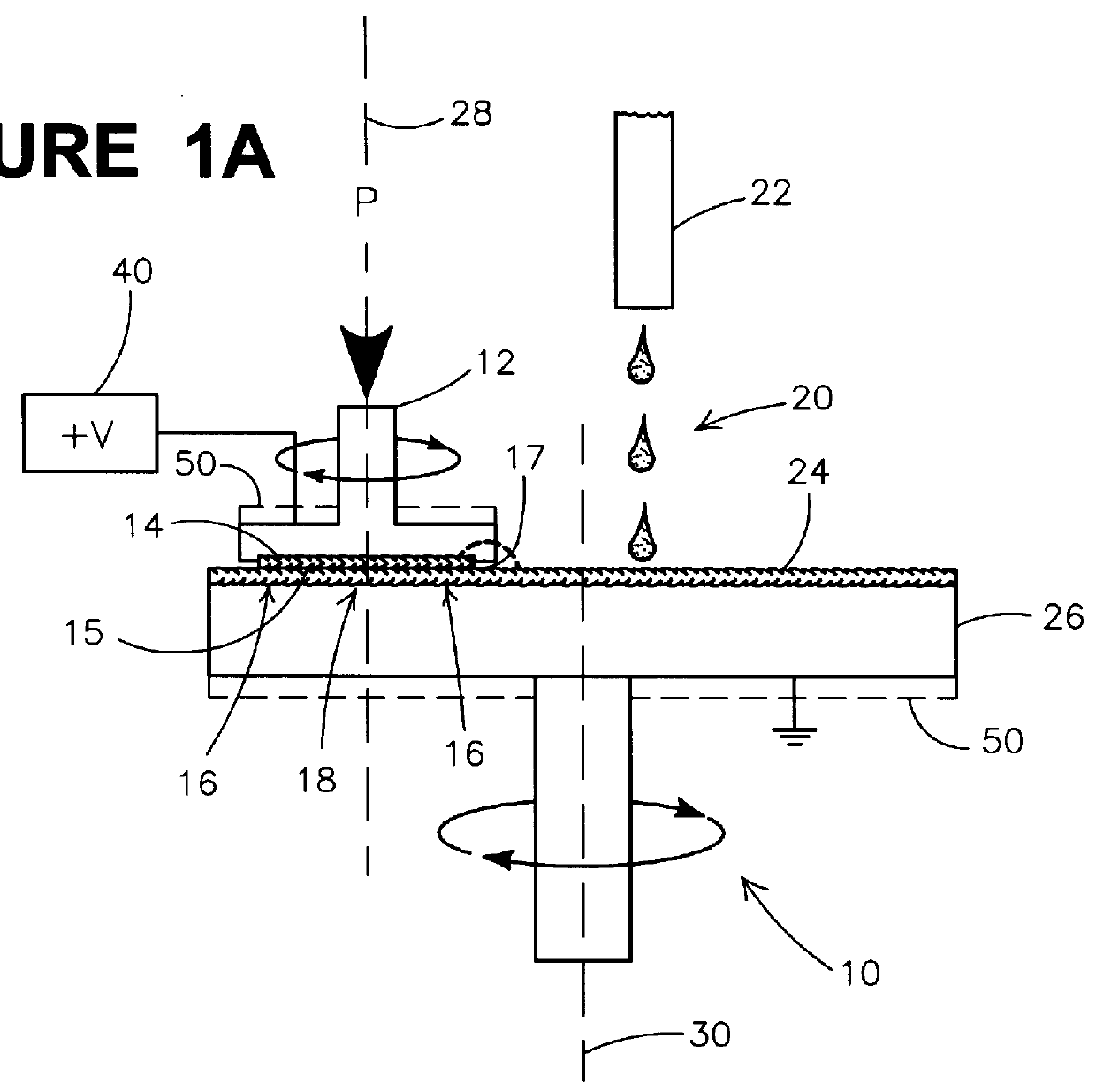
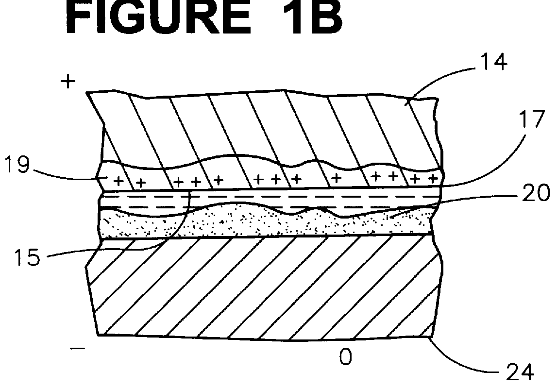
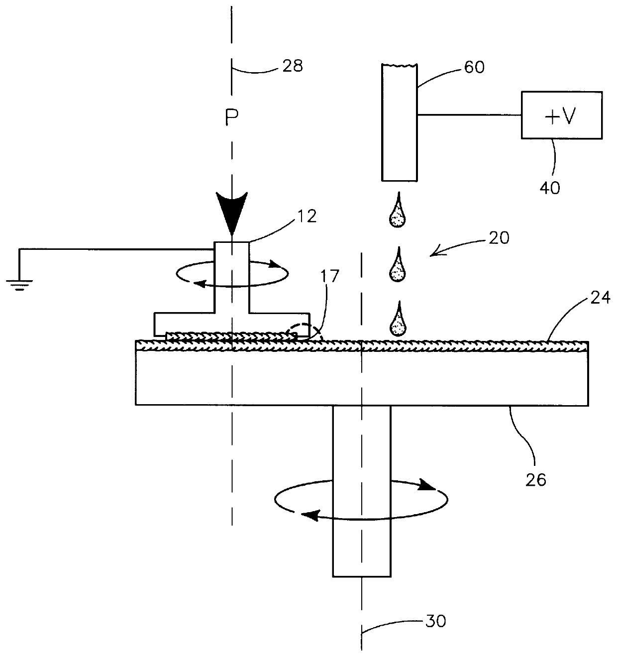
The present invention shall be described with reference to FIGS. 1-4. As used herein, the term substrate assembly includes wafers and any substrate supported structure, i.e., such as a semiconductor substrate or any other substrate having one or more layers or structures formed thereon. Both terms are to be understood as including silicone-on-sapphire (SOS) technology, silicon-on-insulator (SOI) technology, doped and undoped semiconductors, epitaxial layers of silicon supported by a base semiconductor, as well as any other semiconductor based structures well known to one skilled in the art. Furthermore, when a reference is made to a wafer or a substrate assembly in the following description, previous process steps may have been utilized to form regions / junctions / lines, such as metallization lines, insulative layers, etc., in or on a structure previously formed.

Further as used herein, interfacial tension refers to the tension at the interface between immiscible materials, e.g., a liq...


PUM

PropertyMeasurementUnit
electrical potentialaaaaaaaaaa
interfacial tensionaaaaaaaaaa

Abstract

A surface treatment method for use in integrated circuit fabrication includes providing a substrate assembly having a surface. A liquid is provided adjacent the surface resulting in an interface therebetween. An electrical potential difference is applied across the interface and the surface is treated as the electrical potential difference is applied across the interface. The liquid may be a planarization liquid when the treatment of the surface includes planarizing a substrate assembly or the liquid may be a coating material when the treatment of the surface includes applying a coating material on the surface.

Description

FIELD OF THE INVENTIONThe present invention relates to methods and systems for use in integrated circuit fabrication. More particularly, the present invention relates to the use of electrocapillarity in the treatment of wafer surfaces, e.g., planarization, coating, etc.BACKGROUND OF THE INVENTIONIn semiconductor wafer processing, various surface treatment steps are commonly performed. For example, such surface treatment may include application of a coating on the wafer surface or planarizing an exposed wafer surface prior to subsequent processing steps.Planarization, such as chemical-mechanical planarization (CMP), is typically performed to achieve a planar surface over a wafer, sometimes referred to as "global planarity." Typically, the planarization process involves a rotating wafer holder that holds a wafer. A slurry is applied to a rotating table or platen which has a polishing pad thereon. The polishing pad is applied to the wafer at a certain pressure to perform the planarizat...

Claims


Application Information

Patent Timeline
Patent Type & Authority Patents(United States)
IPC IPC(8): H01L21/00
CPCB24B37/042G03F7/162H01L21/31053H01L21/6715
Inventor GLASS, THOMAS R.
Owner MICRON TECH INC
Why Eureka
Try Eureka