Wide band and low driving voltage optical modulator with an improved dielectric buffer layer

a dielectric buffer layer and optical modulator technology, applied in the field of wide band and low driving voltage optical modulators with an improved dielectric buffer layer, can solve the problems of loss of strips, loss due to higher mode propagation, and difficulty in meeting the requirements of driving voltage reduction and widening the bandwidth concurrently, so as to reduce driving voltage and widen the bandwidth

Inactive Publication Date: 2000-02-01
NEC CORP
View PDF7 Cites 17 Cited by
  • Summary
  • Abstract
  • Description
  • Claims
  • Application Information

AI Technical Summary

Benefits of technology

The present invention provides a dielectric buffer layer extending over an optical waveguide and extending under an electrode which applies an electric field through the dielectric buffer layer to the optical waveguide for causing the optical waveguide to vary in refractive index profile in linear-proportion to an intensity of the electric field thereby causing a phase shift of a light which is on propagation in the optical waveguide. It is important for the present invention that the dielectric buffer layer varies in thickness whereby an overlap integral of a profile of the electric field and an optical mode field profile at a thinner portion of the dielectric buffer layer is larger than that at a thicker portion of the dielectric buffer layer, and whereby a difference of an effective microwave refractive index from an optical refractive index at the thicker portion is smaller than that at the thinner portion.
It is preferable that at least the above part of the dielectric buffer layer varies in thickness in two dimensional directions so that variation in thickness of the dielectric buffer layer appears continuously and gradually at least in a direction, along which the light is propagating. In order to drop the driving voltage and widen the bandwidth concurrently, it is more effective to very the thickness of the dielectric buffer layer continuously and gradually at least in a direction, along which the light is propagating. Continuous and gradual variations in thickness of the dielectric buffer layer through which an electric field is applied to the optical waveguide are desirable rather than the discontinuous or rapid variation in thickness of the dielectric buffer layer.

Problems solved by technology

Namely, it was difficult to satisfy the requirements for reduction in the driving voltage and widening the bandwidth concurrently.
a) Loss of strip line conductance which is a function of placement of electrode, resistivity of electrode material and parameters of dielectric buffer layer;
b) Dielectric loss which is a function of dielectric constant of LiNbO.sub.3 substrate and a loss tangent "tan .delta.";
c) Loss due to higher mode propagation;
d) Loss due to curvature or tapering of the strip line;
e) Loss due to impedance mismatch between 50.OMEGA. light source and load; and
f) Loss due to mounting package and outside package which includes loss due to connector and connector strip line contact.
Notwithstanding, it is only a surface impression that it seems inconsistent requirements to satisfy both requirements for reducing the driving voltage and widening the bandwidth concurrently.

Method used


Image

  • Wide band and low driving voltage optical modulator with an improved dielectric buffer layer
  • Wide band and low driving voltage optical modulator with an improved dielectric buffer layer
  • Wide band and low driving voltage optical modulator with an improved dielectric buffer layer

Examples


first embodiment

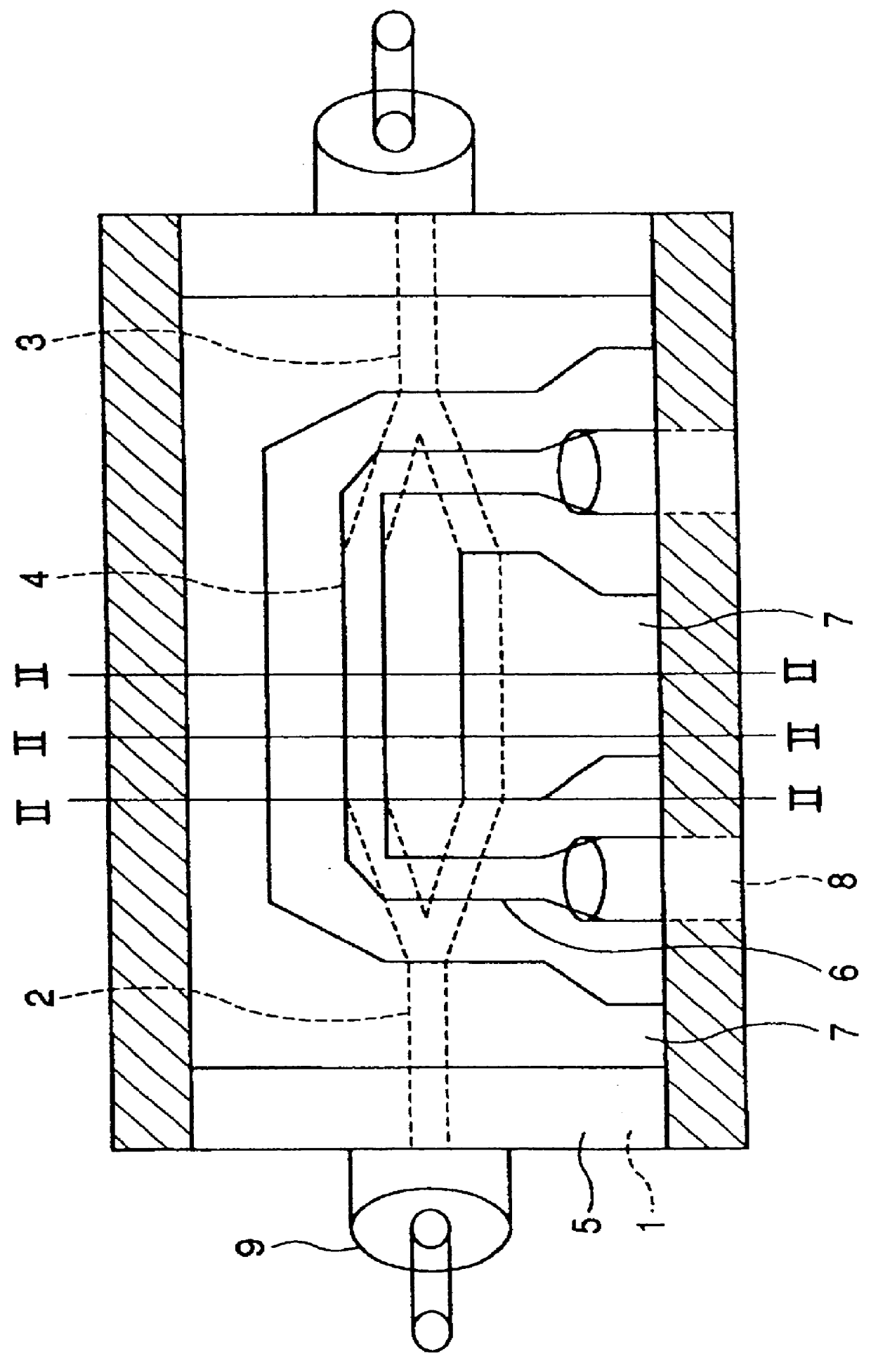
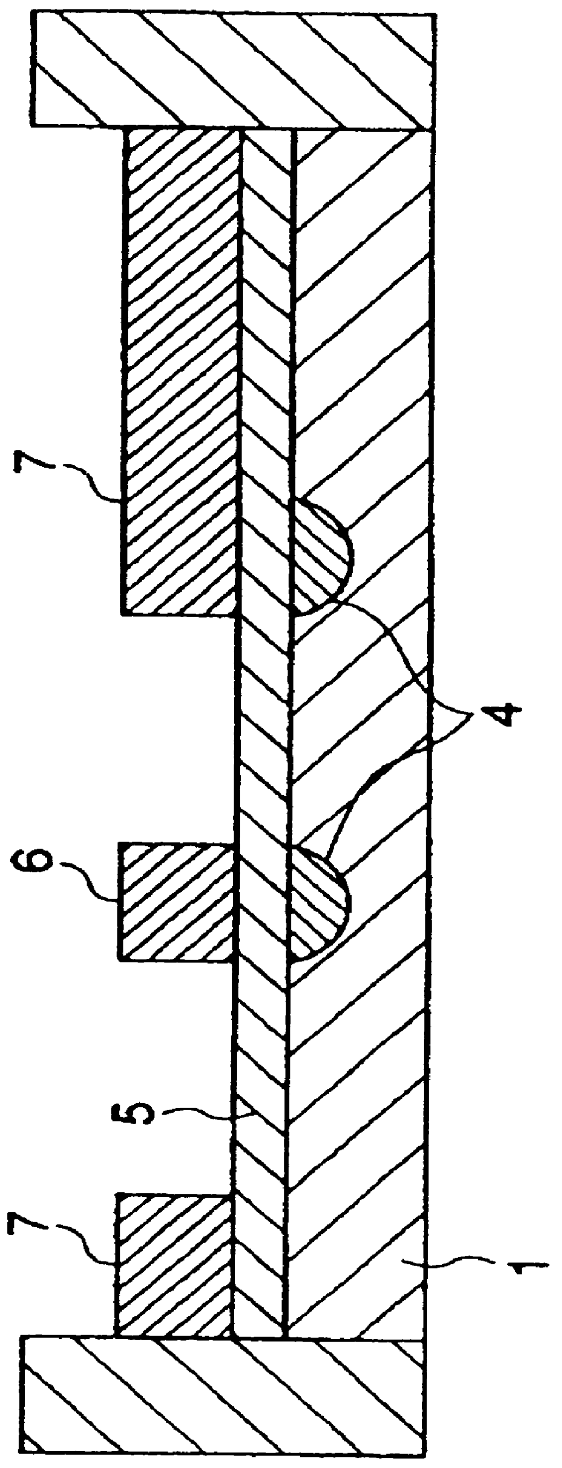
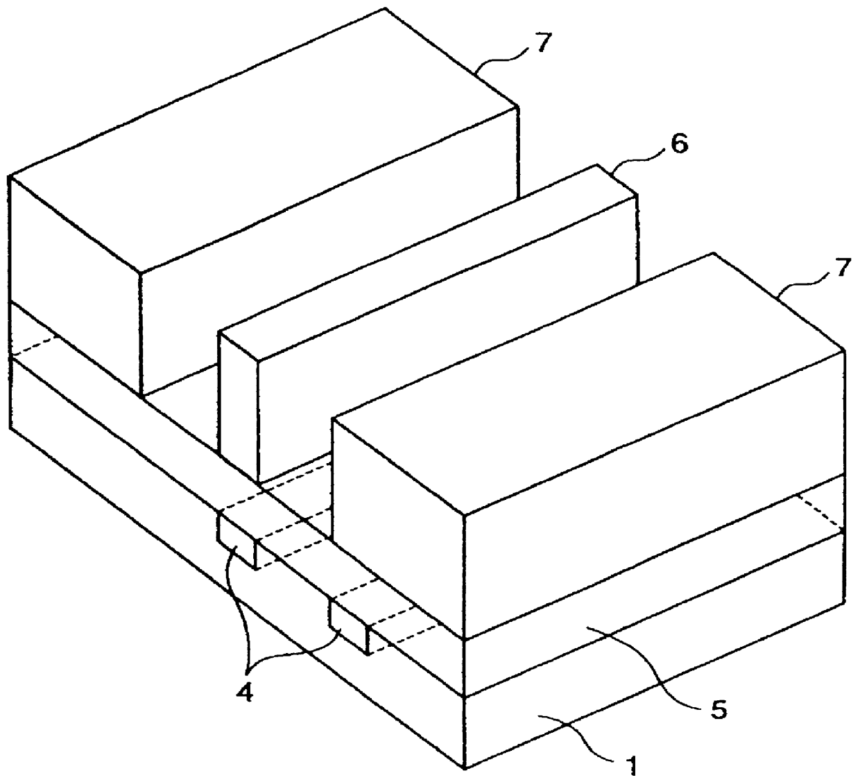
A first embodiment according to the present invention will be described in detail with reference to FIGS. 10, 11A, 11B, 11C, 12 and 13. FIG. 10 is a plane view illustrative of a novel Mach-Zehnder optical modulator including an improved dielectric buffer layer which varies in thickness. FIG. 11A is a cross sectional elevation view illustrative of a novel Mach-Zehnder optical modulator taken along line XIA--XIA in FIG. 10. FIG. 11B is a cross sectional elevation view illustrative of a novel Mach-Zehnder optical modulator taken along line XIB--XIB in FIG. 10. FIG. 11C is a cross sectional elevation view illustrative of a novel Mach-Zehnder optical modulator taken along line XIC--XIC in FIG. 10. FIG. 12 is a schematic perspective view illustrative of the first novel Mach-Zehnder optical modulator of FIG. 10. FIG. 13 is a schematic perspective view illustrative of the first novel Mach-Zehnder optical modulator of FIG. 10, wherein electrodes are displaced to illustrate well the variation...

second embodiment

A second embodiment according to the present invention will be described in detail with reference to FIGS. 15, 16A, 16B and 16C. FIG. 15 is a plane view illustrative of a novel Mach-Zehnder optical modulator including an improved dielectric buffer layer which varies in thickness. FIG. 16A is a cross sectional elevation view illustrative of a novel Mach-Zehnder optical modulator taken along line XVIA--XVIA in FIG. 15. FIG. 16B is a cross sectional elevation view illustrative of a novel Mach-Zehnder optical modulator taken along line XVIB--XVIB in FIG. 15. FIG. 16C is a cross sectional elevation view illustrative of a novel Mach-Zehnder optical modulator taken along line XVIC--XVIC in FIG. 15.

A crystal substrate 1, for example, a LiNbO.sub.3 substrate was prepared which is capable of causing electro-optical effects. A titanium film strip was formed on a top surface of the crystal substrate 1, wherein the titanium film strip comprises two straight arms and two Y-shaped portions coupled...

third embodiment

A third embodiment according to the present invention will be described in detail with reference to FIGS. 17, 18A, 18B and 18C. FIG. 17 is a plane view illustrative of a novel Mach-Zehnder optical modulator including an improved dielectric buffer layer which varies in thickness. FIG. 18A is a cross sectional elevation view illustrative of a novel Mach-Zehnder optical modulator taken along line XVIIIA--XVIIIA in FIG. 17. FIG. 18B is a cross sectional elevation view illustrative of a novel Mach-Zehnder optical modulator taken along line XVIIIB--XVIIIB in FIG. 17. FIG. 18C is a cross sectional elevation view illustrative of a novel Mach-Zehnder optical modulator taken along line XVIIC--XVIIC in FIG. 17.

A crystal substrate 1, for example, a LiNbO.sub.3 substrate was prepared which is capable of causing electro-optical effects. A titanium film strip was formed on a top surface of the crystal substrate 1, wherein the titanium film strip comprises two straight arms and two Y-shaped portion...


PUM


Abstract

An optical modulator has a dielectric buffer layer extending over an optical waveguide and extending under an electrode which applies an electric field through the dielectric buffer layer to the optical waveguide for causing the optical waveguide to vary in refractive index profile in linear-proportion to an intensity of the electric field thereby causing a phase shift of a light which is on propagation in the optical waveguide, wherein the dielectric buffer layer varies in thickness whereby an overlap integral of a profile of the electric field and an optical mode field profile at a thinner portion of the dielectric buffer layer is larger than that at a thicker portion of the dielectric buffer layer, and whereby a difference of an effective microwave refractive index from an optical refractive index at the thicker portion is smaller than that at the thinner portion.

Description

The present invention relates to an optical device, and more particularly to an optical device such as waveguide optical modulators and waveguide optical switches used in high speed optical communications, optical switching networks, optical information processing, image processing and other various optical systems.The waveguide optical modulators and waveguide optical switches are extremely important for realizing the high speed optical communications, optical switching networks, optical information processing, image processing and other various optical systems.The waveguide optical modulators may be fabricated on a few kinds of attracted substrates. The studies of the waveguide optical devices have been likely to focus on LiNbO.sub.3 substrate or semiconductor substrates such as GaAs substrate. A low loss strip type optical waveguide may be formed in an upper region of the LiNbO.sub.3 substrate by selective diffusion of titanium into the upper region of the LiNbO.sub.3 substrate.T...

Claims


Application Information

Patent Timeline
Patent Type & Authority Patents(United States)
IPC IPC(8): G02F1/01G02F1/035G02F1/225
CPCG02F1/0356G02F1/2255G02F2201/07
Inventor MADABHUSHI, RANGARAJ
Owner NEC CORP
Why Eureka
Try Eureka