
Bias circuit for transconductance amplifier

a bias circuit and amplifier technology, applied in the field of integrated circuits, can solve the problems of not necessarily valid assumption, significant errors in the bias scheme, and the inability to bias the transconductance stage for proper circuit operation

Inactive Publication Date: 2000-02-08
LUCENT TECH INC
View PDF3 Cites 57 Cited by
  • Summary
  • Abstract
  • Description
  • Claims
  • Application Information

AI Technical Summary

Problems solved by technology

At low power supply voltages required by some applications, it may become impossible to bias the transconductance stage for proper circuit operations.
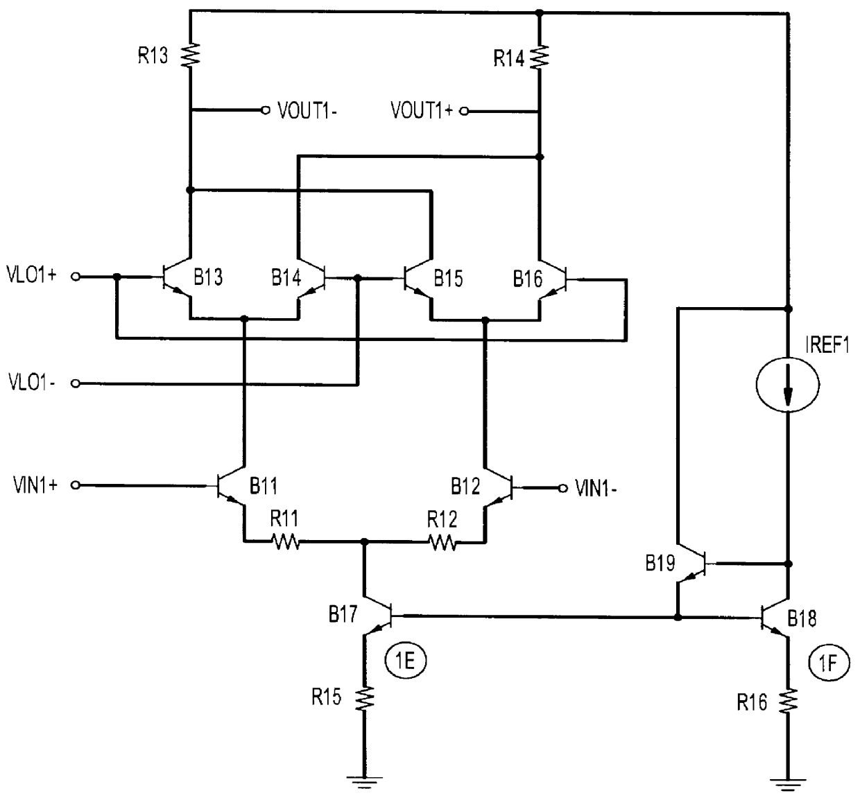
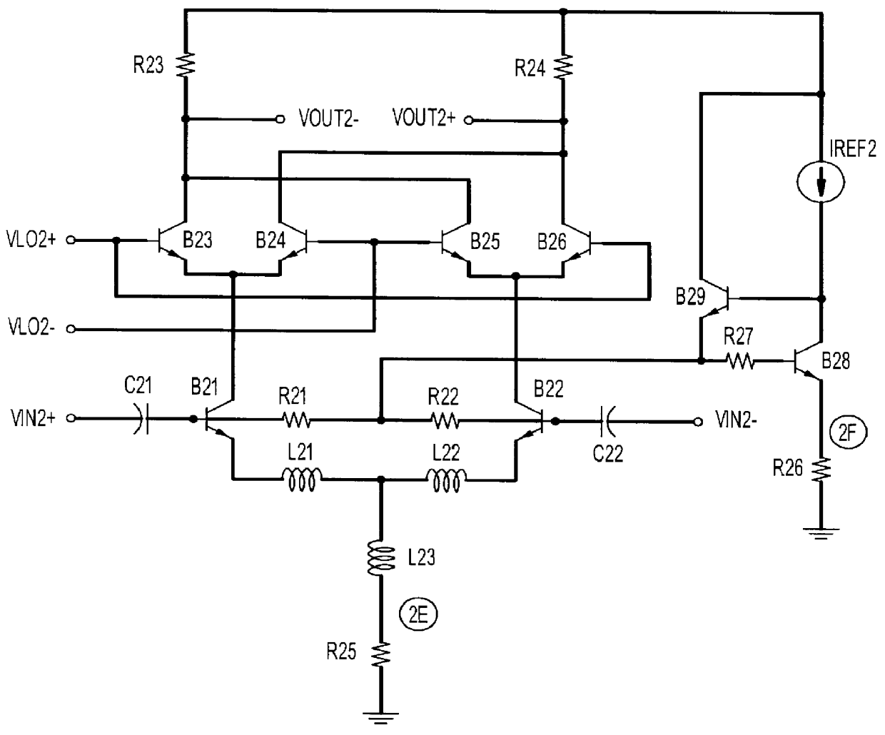
A problem exists with the circuit in FIG. 2 that can be explained by comparing the bias circuit in FIG. 1 to the bias circuit of FIG. 2.
However, this is not necessarily a valid assumption for the circuit shown in FIG. 2.
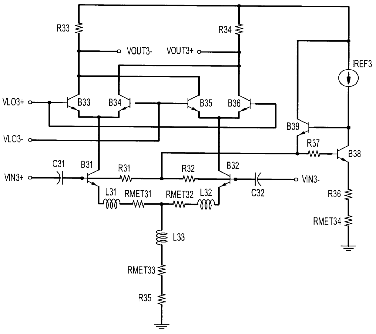
If the resistance of the inductors is large enough compared to the value of resistor R25, significant errors will occur in the bias scheme.
The area needed to implement such a resistor can be very large and can add significant cost to an integrated circuit.

Method used


Image

  • Bias circuit for transconductance amplifier
  • Bias circuit for transconductance amplifier
  • Bias circuit for transconductance amplifier

Examples


Embodiment Construction

FIG. 4 shows a circuit that addresses the interconnection problem introduced by the resistance of the inductors and any interconnect resistance in series with the inductors. In this circuit, only the transconductance amplifier portion of the circuit has been shown, since this solution is applicable to any transconductance stage, not just those used as part of a mixer, as in the circuits of FIGS. 1-3.

In the circuit of FIG. 4, an operational amplifier is used in a feedback loop to establish the desired bias conditions. A current IREF4 is driven into a resistor R46 to establish a reference voltage at the positive input to the operation amplifier OPA41. The negative input is tied to the current sensing resistor R45. The feedback loop drives the voltage at node 4D to be the level required to make the voltage at node 4E equal to the reference voltage at node 4F. Since the voltages at nodes 4E and 4F are forced to be equal, the current through resistor R45 can be set to M times the referen...


PUM


Abstract

In low-voltage circuits, there is often insufficient voltage to use a current source to bias a transconductance amplifier stage. This is particularly true in mixers where a switching circuit must be stacked on top of the transconductance input stage. One way around this problem is to get "double-duty" out of the input differential pair, using it both for gain stage and for DC bias. This is done by AC coupling in a high-frequency input signal, while using a low-frequency, DC-coupled circuit to establish the proper bias level. One common technique is to use a simple current mirror scheme to establish the DC level. Proper biasing using this technique requires good matching of resistance. In some implementations of transconductance amplifiers, particularly those that use inductors as degeneration elements, series resistance of the inductor and interconnect resistance can cause significant errors in the bias current. This invention addresses that problem by using an operational amplifier with a current-sensing resistor and a low-frequency feedback loop to compensate automatically for any resistance errors. The operational amplifier drives the feedback voltage (generated in accordance with the sensed voltage at the current-sensing resistor and applied to one input of the operational amplifier) towards a reference voltage that is applied to the other input of the operational amplifier to bias the transistor(s) in the transconductance amplifier for desired operating conditions.

Description

1. Field of the InventionThe present invention relates to integrated circuits, and, in particular, to transconductance amplifiers.2. Description of the Related ArtA transconductance amplifier converts an input voltage signal into an output current signal, where output current is proportional to the input voltage. Conventional transconductance amplifiers have a transistor to provide amplification of the input signal and a DC bias circuit to bias the transistor for operations. In order to save power, e.g., in many battery-operated devices, circuits having transconductance amplifiers may be required to operate from low supply voltages. Typically, a certain minimum voltage is required in order to bias a transconductance amplifier for proper operation. As supply voltages decrease, the available voltage approaches, or in some cases drops below, the minimum voltage needed to bias the circuit.FIG. 1 shows a traditional Gilbert cell mixer implementation that is used to illustrate this proble...

Claims


Application Information

Patent Timeline
IPC IPC(8): H03F1/30H03F3/45H03D7/14
CPCH03D7/1433H03F1/302H03F3/45085H03F3/45089H03F3/45538H03D7/1441H03D7/145H03D7/1458H03D7/1491H03F2200/372H03F2203/45311H03F2203/45386H03F2203/45498H03F2203/45501H03F2203/45542H03F2203/45544H03F2203/45561H03F2203/45702H03D2200/0033H03D2200/0043
Inventor ASHBY, KIRK B.DAVIS, PAUL C.WOMAC, MICHAEL D.
Owner LUCENT TECH INC
Learn More