Synchronous delay circuit

a delay circuit and synchronous technology, applied in the field of synchronous delay circuits, can solve the problems of high inefficiency, difficult design of clock dummy delay circuits, and insufficient exploiting circuit merits

Inactive Publication Date: 2000-06-13
RENESAS ELECTRONICS CORP
View PDF4 Cites 38 Cited by
  • Summary
  • Abstract
  • Description
  • Claims
  • Application Information

AI Technical Summary

Problems solved by technology

Thus, the problem is raised that, by adding the function of Duty50 and double frequency, it is not possible to exploit the merit proper to the circuit sufficiently.
With devices in which the amount of clock delay differs depending upon the wiring design used in the chip, designing the clock dummy delay circuit is difficult and it is necessary to design the dummy delay circuit after the wiring is laid out.
This is highly inefficient.
This is uneconomical.

Method used


Image

  • Synchronous delay circuit
  • Synchronous delay circuit
  • Synchronous delay circuit

Examples


embodiment 1

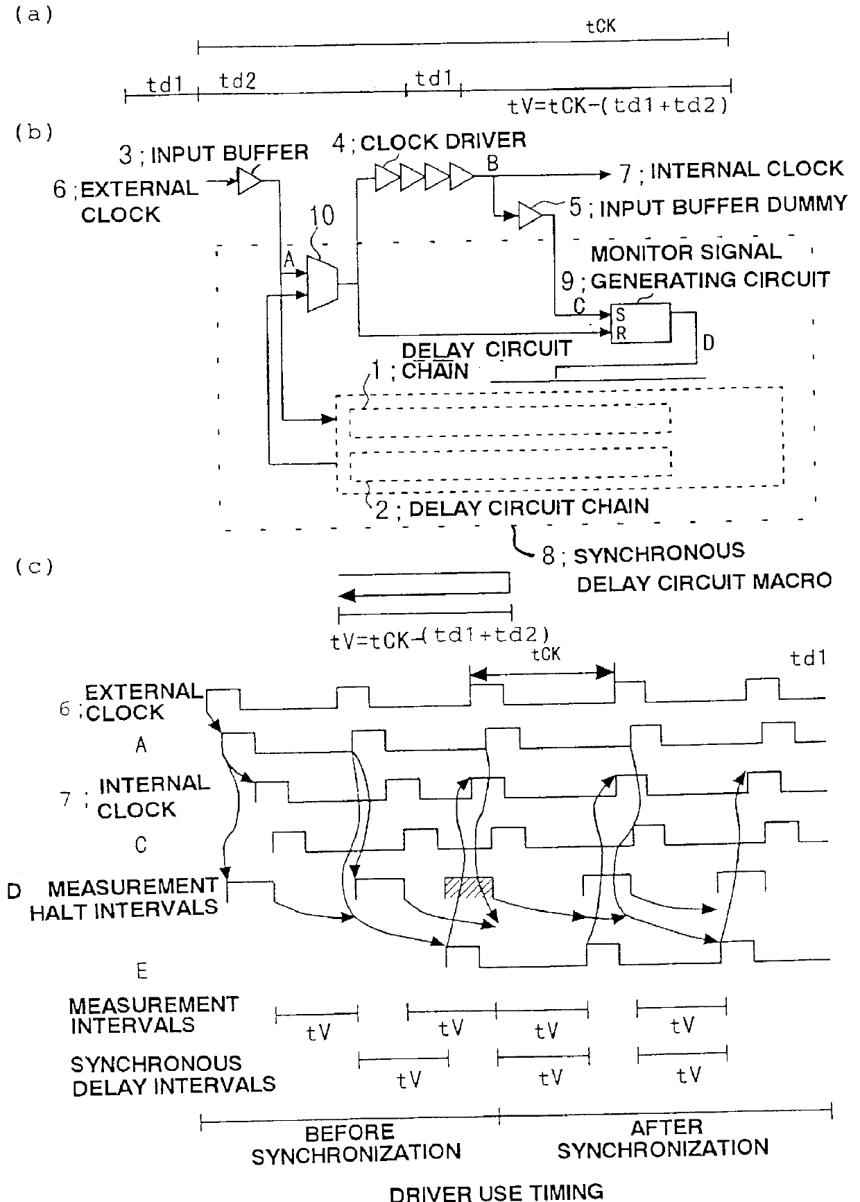
FIG. 1 shows a constitution of a synchronous delay circuit according to a first embodiment of the present invention and a timing chart. Referring to FIG. 1, the first embodiment of the present invention includes a synchronous delay circuit made up of a delay circuit chain 1 for measuring a pre-set time interval, a delay circuit chain 2 for reproducing the measured delay time, the input buffer 3 and the clock driver 4. The clock driver 4 furnishes internal clocks 7 to an internal circuit (sequencing circuit), not shown. An input buffer dummy 5 is configured similarly to the input buffer 4 and has the same delay time.

An output A of the input buffer 3 is sent to an input end of a switch 10 (changeover unit) and to the delay circuit chain 1 for measuring the period. The other input end of the switch 10 is entered an output of the delay circuit chain 2 for reproducing the delay. An output of the switch 10 is sent to an input of the clock driver 4 and to a reset terminal of a monitor sign...

fourth embodiment

FIG. 28 is a timing chart for illustrating the present invention.

FIG. 29 shows an example of the structure of a delay circuit chain in the fourth embodiment of the present invention.

FIG. 30 shows a typical structure of a delay circuit chain in the fourth embodiment of the present invention.

FIG. 31 shows another typical structure of the delay circuit chain in the fourth embodiment of the present invention.

FIG. 32 shows still another typical structure of the delay circuit chain in the fourth embodiment of the present invention.

FIG. 33 shows yet another typical structure of the delay circuit chain in the fourth embodiment of the present invention.

Further, a monitor signal generating circuit 9 for outputting a monitor signal D in the period of time during which a pulse is propagating through the clock driver 4 and input buffer dummy 5 is constituted by an RS flip-flop or the like. In a case where the time (td1+td2), which is obtained by adding the amounts of delay in the clock driver 4 ...

first example

[FIRST EXAMPLE]

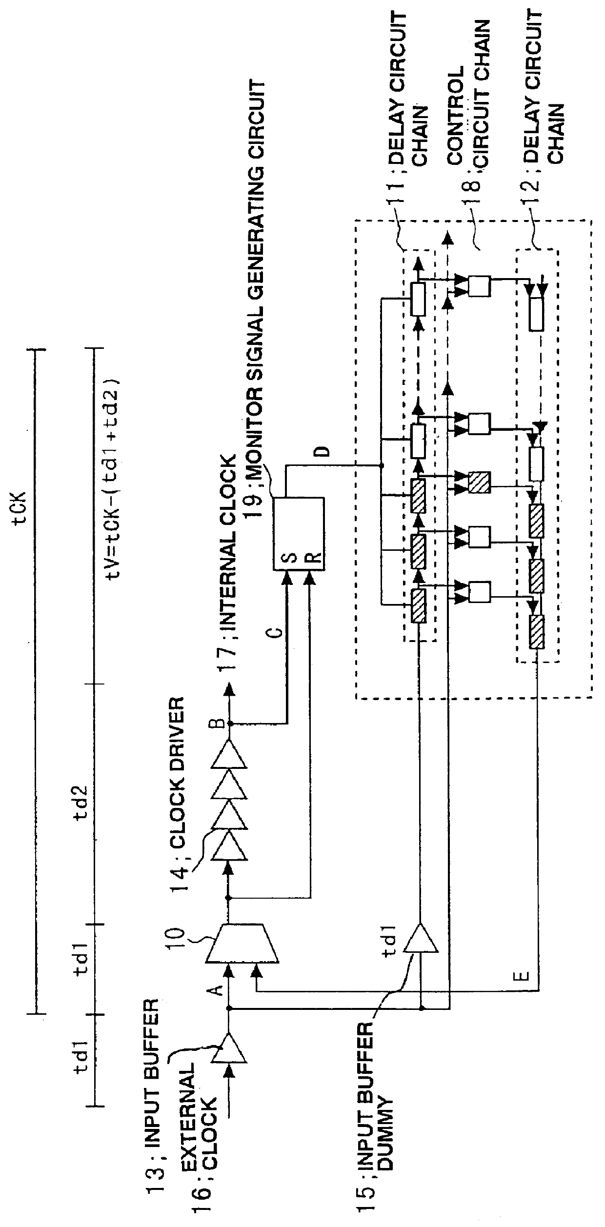
FIG. 2 is a diagram showing a circuit arrangement according to a first example of the present invention.

This example employs a scheme in which a delay circuit chain 11 for measuring the clock period tCK and a delay circuit chain 12 for reconstructing the measured period are arranged in mutually opposing directions.

This scheme in which the delay circuit chain 11 and the delay circuit chain 12 for reconstructing the measured period are arranged in opposite directions is such that a clock pulse propagates through the delay circuit chain 11 and then is transferred to the delay circuit chain 12 via a control circuit chain 18 when the next clock pulse is output by an input buffer 13. This arrangement corresponds to the scheme set forth in Japanese Patent Application Laid-Open No. 8-137091 described above in connection with FIG. 10.

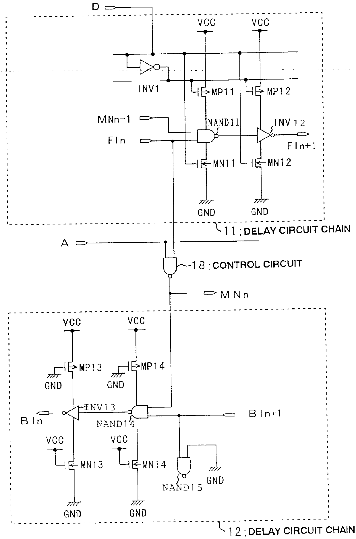
More specifically, the arrangement shown in FIG. 2 comprises the delay circuit chain 11 capable of extracting an output from any position along t...


PUM


Abstract

A synchronous delay circuit contains a first delay circuit for propagating a pulse for a fixed period of time, a second delay circuit for passing the pulse over a length proportional to the length of the first delay circuit along the path that the pulse propagated, and a circuit for outputting a monitor signal when a clock period is propagating through a clock driver. The first delay circuit measures a clock period tCK, and the second delay circuit reconstructs the measured clock period. External clock signals travel through a path from an input buffer through a first switch of a clock driver. The time corresponding to a delay time of the input buffer (td1) and a delay time of the clock divider (td2) is subtracted from the clock period tCK producing a delay circuit with a delay of tCK-(td1+td2). When the clock pulse passes through the delay circuit whose delay is tCK-(td1+td2), the internal clock delay becomes equal to the clock cycle tCK. Thus, the internal clock is free of clock skew.

Description

This invention relates to a semiconductor integrated circuit and, more particularly, to a synchronous delay circuit for controlling a clock signal.Owing to their circuit simplicity and small current consumption, synchronous delay circuits that eliminate clock skew in a short synchronization time find use in high-speed clock synchronizing circuits. Reference may be had to the following literature describing such synchronous delay circuits:(1) Japanese Patent Kokai publicaiton No. JP-A-8-237091;(2) "Skew Minimization Technique for 256 M-bit Synchronous DRAM and Beyond", by Jin-Man Han, et al., 1996 Symp. on VLSI Circ., pp. 192.about.193;(3) "Clock Buffer Chip with Absolute Delay Regulation Over Process and Environment Variations", by Richard B. Watson et al., Proc. of IEEE 1992 (Custom Integrated Circuits Conference), 25.2; and(4) "Digital Delay Locked Loop and Design Technique for High-Speed Synchronous Interface", IEICE TRANS. ELECTRON., VOL. E79-C, No. 6, June, 1996, pp. 798.about....

Claims


Application Information

Patent Timeline
Patent Type & Authority Patents(United States)
IPC IPC(8): H03K5/135H03K5/13
CPCH03K5/135H03K5/133
Inventor SAEKI, TAKANORI
Owner RENESAS ELECTRONICS CORP
Why Eureka
Try Eureka