Method for milling a transmission electron microscope test slice

a technology of transmission electron microscope and test slice, which is applied in the direction of material analysis using wave/particle radiation, instruments, nuclear engineering, etc., can solve the problems of poor resolution, insufficient thickness of test slice, and insufficient thickness around the bottom region

Inactive Publication Date: 2000-06-27
UNITED MICROELECTRONICS CORP
View PDF3 Cites 42 Cited by
  • Summary
  • Abstract
  • Description
  • Claims
  • Application Information

AI Technical Summary

Problems solved by technology

A scanning electron microscope (SEM) is one of the diagnostic tools used to observe the cross-sectional surface but its resolution is poor when integration density is high, as is the case with the VLSI device.
Because of the application of the TEM, the production of a test slice with an allowed thickness becomes an important issue.
Since the thickness is progressively wider, the thickness around the bottom region may be too thick even though the top region has a suitable thickness.
If the thickness is too thick, TEM can not effectively penetrate the TEM observable wall, and then TEM diagnosis is therefore limited only on the top region.
This thickness of 0.1 microns cannot be easily controlled.
If over-milling occurs, the test slice is then damaged.
On the contrary, if insufficient milling occurs, the test slice is then not suitable for TEM diagnoses.
It becomes an important issue to choose a proper type of milling stop signal in order to obtain a TEM test slice with a proper uniform thickness.

Method used


Image

  • Method for milling a transmission electron microscope test slice
  • Method for milling a transmission electron microscope test slice
  • Method for milling a transmission electron microscope test slice

Examples


Embodiment Construction

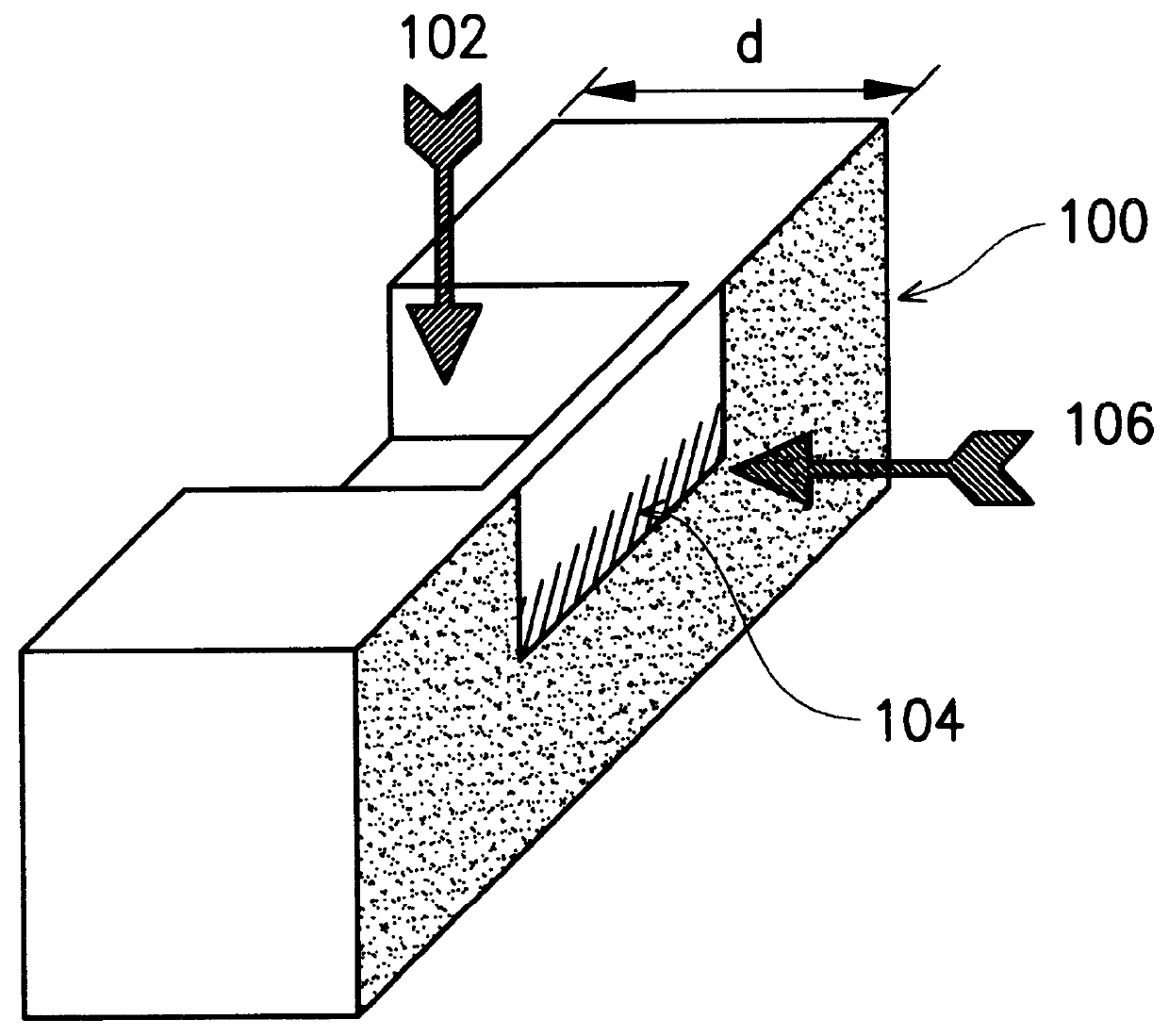
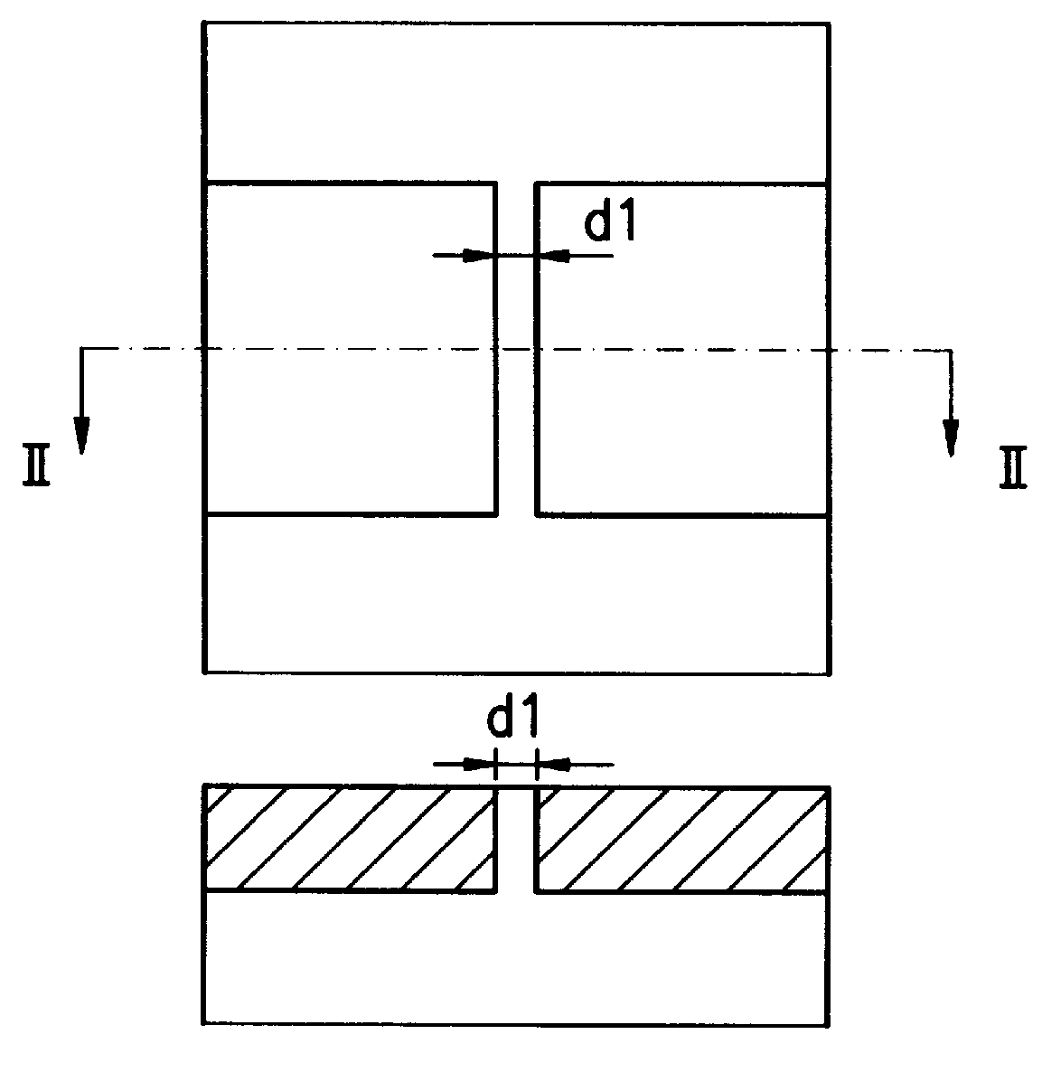
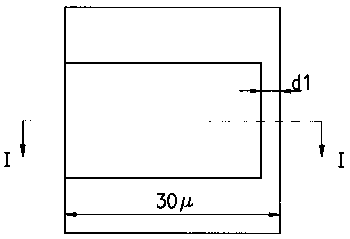
The TEM test slice has an original thickness of about 30 microns. A suitable range can be about 25-35 microns. One can perform the steps shown in FIG. 3A and FIG. 3B until the step A4, at which point a small current of FIB is used to mill the TEM test slice. Then several steps are performed according to the invention. First, at this stage, a slanting angle .theta. described in FIG. 4 is determined by, for example, measuring it. This slanting angle .theta. is intrinsic to the FIB milling process.

FIG. 5A and FIG. 5B are cross-sectional views schematically illustrating a FIB milling method for a TEM test slice, according to a preferred embodiment of the invention. In FIG. 5A, a working flat plate 505, which is used to hold the TEM test slice, is tilted with an angle .theta., also called the tilt angle, substantially equal to the intrinsic slanting angle, in counterclockwise direction. One side surface of a TEM observable wall 51Oa is thereby parallel to the FIB incident direction. Next...


PUM

PropertyMeasurementUnit
heightaaaaaaaaaa
thicknessaaaaaaaaaa
thicknessaaaaaaaaaa

Abstract

A focused ion beam (FIB) is used to mill a test slice to form an observable wall for a transmission electron microscope (TEM). A slanting angle theta of the observable wall surface is automatically formed. The method for milling the test slice includes the following steps: The first step is to measure the slanting angle theta . The next step is to tilt the test slice with the slanting angle theta in both a counterclockwise direction and a clockwise direction and to perform FIB milling so that the TEM observable wall has a uniform thickness. Furthermore, during the FIB milling, an aperture in the TEM observable wall serves as a milling stop signal.

Description

This application claims the priority benefit of Taiwan application serial no. 87109768, filed Jun. 18, 1998, the full disclosure of which is incorporated herein by reference.1. Field of the InventionThis invention relates to a method for milling a test slice, and more particularly to a method of milling a transmission electron microscope (TEM) test slice, which has a uniform thickness.2. Description of Related ArtIn a failure analysis of a vary-large-scale-integration (VLSI) device, the analysis of a cross-sectional surface has been accepted as an effective diagnostic technology. A scanning electron microscope (SEM) is one of the diagnostic tools used to observe the cross-sectional surface but its resolution is poor when integration density is high, as is the case with the VLSI device. The TEM is another diagnostic tool, which has been introduced to gradually replace the SEM. In order to maintain the reliability of the VLSI device and streamline its production, the TEM is becoming m...

Claims


Application Information

Patent Timeline
Patent Type & Authority Patents(United States)
IPC IPC(8): G01N1/28G01Q30/20
CPCG01N1/286H01J2237/3114H01J2237/282H01J2237/26
Inventor TSAI, CHING-LONG
Owner UNITED MICROELECTRONICS CORP
Why Eureka
Try Eureka