Methods for reducing the effects of power supply distribution related noise

a technology of power supply distribution and noise reduction, applied in the field of integrated circuits, can solve the problems of reducing the power consumption and reducing the power consumption of microprocessors and vlsi chips. only a limited extent, and the effect of reducing the power consumption of vlsi chips

Inactive Publication Date: 2000-08-29
INTEL CORP
View PDF3 Cites 12 Cited by
  • Summary
  • Abstract
  • Description
  • Claims
  • Application Information

AI Technical Summary

Problems solved by technology

The new generation of microprocessors and VLSI chips generally tend to consume more power than the previous generation.
However, because the effective switching capacitance and the frequency of operation of the VLSI chip are increasing at a high rate from one generation to another, the net effect has been an increase in the power consumption in the VLSI chip.
While reducing the supply voltage V.sub.CC results in power savings, such supply voltage scaling can be done only to a limited extent.
As a result, the parasitic effects of resistances and inductances, in the circuit worsen, thereby increasing the power supply distribution related noise.
The power supply distribution related noise is caused by the voltage drops across the resistors and the inductors.
Furthermore, the supply voltage scaling reduces the noise margin of the circuits on the VLSI chip, which makes the circuits more susceptible to the power supply distribution related noise.
But larger-size MOSFETs will increase the size of the chips, thereby making the prior art method less cost effective.

Method used


Image

  • Methods for reducing the effects of power supply distribution related noise
  • Methods for reducing the effects of power supply distribution related noise
  • Methods for reducing the effects of power supply distribution related noise

Examples


Embodiment Construction

Illustrative embodiments of the invention are described below. In the interest of clarity, not all features of an actual implementation are described in this specification. It will of course be appreciated that in the development of any such actual embodiment, numerous implementation-specific decisions must be made to achieve the developers' specific goals, such as compliance with system-related and business-related constraints, which will vary from one implementation to another. Moreover, it will be appreciated that such a development effort might be complex and time-consuming, but would nevertheless be a routine undertaking for those of ordinary skill in the art having the benefit of this disclosure.

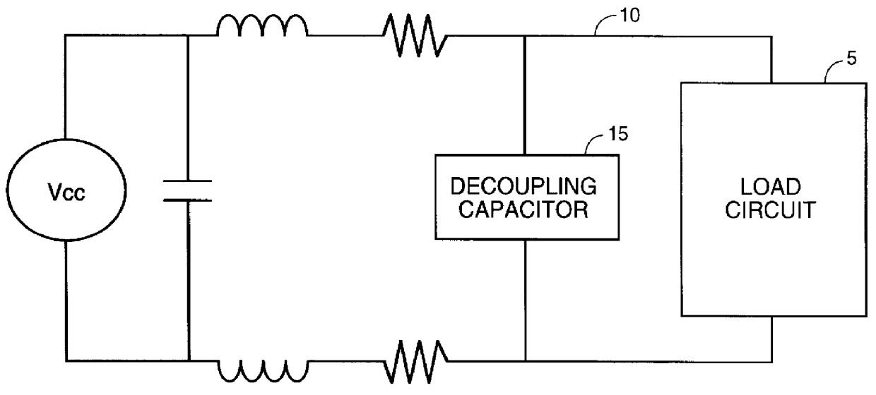
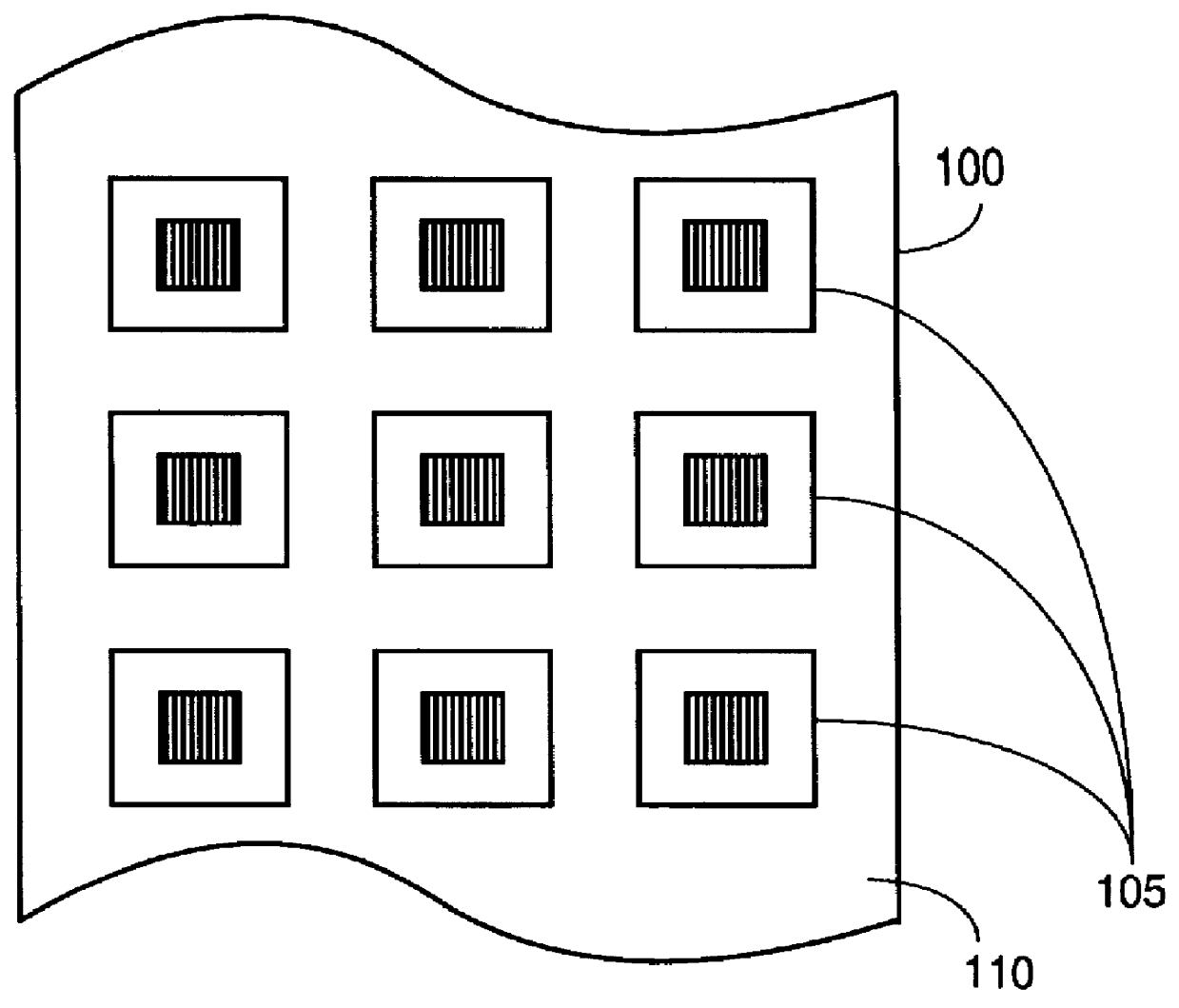
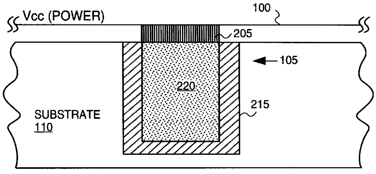
Referring now to the drawings, and in particular to FIG. 2, there is shown a method and apparatus of the present invention for reducing power supply distribution related noise. As shown, FIG. 2 includes a power bus 100 and a plurality of trench capacitors 105 connected in parallel.

The ...


PUM


Abstract

A method is provided for reducing the effects of power supply distribution related noise in an integrated circuit, the integrated circuit having a power supply bus, a ground bus, a DRAM-technology capacitor, and a load circuit. The method includes forming the DRAM-technology capacitor adjacent the load circuit, and connecting the DRAM-technology capacitor directly between the supply voltage bus and the ground voltage bus.

Description

1. Field of the InventionThis invention relates generally to integrated circuits, and, more particularly, to reducing the effects of power supply distribution related noise in integrated circuits.2. Description of the Related ArtThe demand for faster and more powerful personal computers has led to many technological advances in the computer industry, including the development of faster microprocessors and very large scale integration (VLSI) chips. The new generation of microprocessors and VLSI chips generally tend to consume more power than the previous generation.To reduce the power consumption, logic designers have entertained several options, including reducing the supply voltage V.sub.CC. The general trend has been to reduce the supply voltage V.sub.CC by approximately 30 percent per generation, which has resulted in power savings of approximately 50 percent. However, because the effective switching capacitance and the frequency of operation of the VLSI chip are increasing at a ...

Claims


Application Information

Patent Timeline
Patent Type & Authority Patents(United States)
IPC IPC(8): G11C11/4074G11C7/24G11C7/00G11C11/407G11C5/00G11C7/02
CPCG11C5/005G11C5/063G11C5/14G11C7/02G11C7/24G11C11/4074
Inventor BORKAR, SHEKHAR YESHWANT
Owner INTEL CORP
Why Eureka
Try Eureka