Integrated circuit memory cell having a small active area and method of forming same

a memory cell and integrated circuit technology, applied in the field of memory cells, can solve the problems of large size, lower storage densities, and increased manufacturing costs, and achieve the effects of reducing the cost of manufacturing, and reducing the size of the hol

Inactive Publication Date: 2000-09-05
ROUND ROCK RES LLC
View PDF46 Cites 387 Cited by
  • Summary
  • Abstract
  • Description
  • Claims
  • Application Information

AI Technical Summary

Problems solved by technology

Furthermore, DRAMs typically require less area on a die than the other memories, but DRAMs generally do not exhibit the fastest access times. Thus, as can be appreciated due to the many trade-offs between these different memory configurations, the type of memory used greatly depends upon the requirements of the system in which it is used.
Although the memory cells of SRAMs, ROMs, and flash memories do not require refreshing, they suffer from disadvantages, such as lower storage densities, larger size, and greater cost to manufacture.
However, these methods suffer from technological constraints upon the hole size.
The size of the cavity, and therefore the size of the electrodes, achieved through this method is generally unpredictable.

Method used


Image

  • Integrated circuit memory cell having a small active area and method of forming same
  • Integrated circuit memory cell having a small active area and method of forming same
  • Integrated circuit memory cell having a small active area and method of forming same

Examples


Embodiment Construction

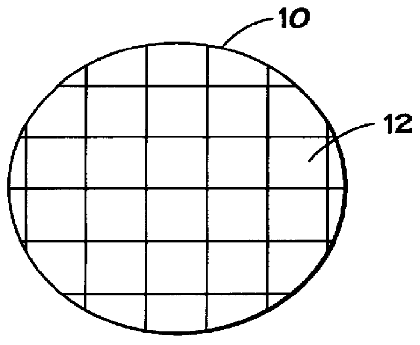
Turning now to the drawings, and referring initially to FIG. 1, a wafer, such as a semiconductor wafer, is illustrated and generally designated by a reference numeral 10. One or more integrated circuits may be fabricated on the wafer 10. The wafer 10 may be separated into a plurality of integrated circuit dies 12, which may be packaged as integrated circuit chips.

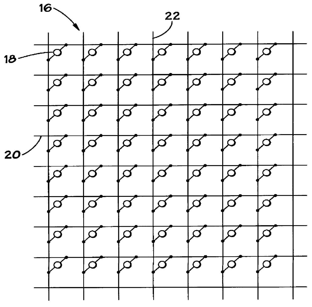
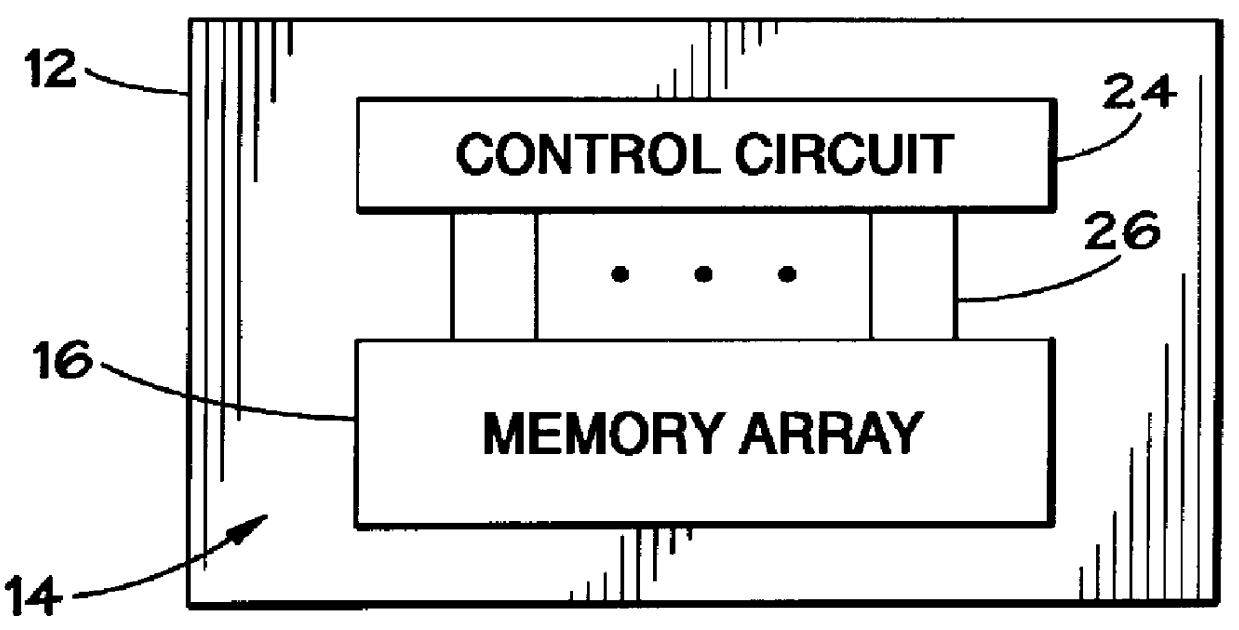
A die 12 may contain an integrated circuit memory 14, such as that illustrated in FIG. 2. The memory 14 may include one or more memory arrays 16. The memory array 16 typically includes a plurality of memory cells 18 that are arranged in generally perpendicular rows and columns, as illustrated in FIG. 3. The memory cells 18 in each row typically share an electrical connection referred to as a word line 20, and the memory cells 18 in each column typically share an electrical connection referred to as a bit line 22. The memory array 16 is coupled to control circuitry 24 by lines 26. The control circuitry 24 accesses each memor...


PUM


Abstract

A method for manufacturing a memory device having a plurality of memory cells. Each memory cell has a non-volatile resistive memory element with a small active area. A plurality of memory cells are formed at selected locations of at least a portion of a semiconductor wafer. To form the memory cells, a lower electrode layer and a memory material layer are deposited over at least a portion of the wafer. Patterns are formed over desired contact locations of the memory material layer and etching is used to remove portions of the memory material layer. The etching step undercuts the patterns and forms memory elements having a protruding contact portion with an apex contact area. The pattern is removed, and an upper electrode is formed and electrically coupled to the contact area. Corresponding access devices and word / bit line conductor grids are provided and coupled to the memory cells.

Description

1. Field of the InventionThe present invention relates generally to memories and, more particularly, to memory cells having chalcogenide memory elements.2. Background of the Related ArtIn the field of integrated circuit memory devices, there is a continuing trend toward memories that have store more information, consume less power, operate faster, take up less space, and cost less to make. While these are often competing interests, memory manufactures strive to make advances in these areas to remain competitive. Thus, the ability to manufacture small memory cells efficiently is crucial in maximizing the performance and cost-efficiency of a memory device.Popular memories today include dynamic random access memories (DRAMs), static random access memories (SRAMs), read only memories (ROMs), and flash memories. Certain basic characteristics are shared by these memories. For example, these memories typically include one or more memory arrays, where each array has a plurality of memory ce...

Claims


Application Information

Patent Timeline
Patent Type & Authority Patents(United States)
IPC IPC(8): H01L45/00H01L27/10
CPCH01L27/101H01L45/06H01L45/1233H01L27/2409H01L45/144H01L45/1675H01L45/1691H01L45/1246H10B63/20H10N70/231H10N70/828H10N70/826H10N70/8828H10N70/068H10N70/063
Inventor ZAHORIK, RUSSELL C.
Owner ROUND ROCK RES LLC
Why Eureka
Try Eureka