SRAM layout for relaxing mechanical stress in shallow trench isolation technology and method of manufacture thereof

a technology of mechanical stress and layout, which is applied in the direction of semiconductor devices, semiconductor/solid-state device details, electrical devices, etc., can solve the problems of creating leakage paths and mechanical stress being a problem

Inactive Publication Date: 2000-09-12
TAIWAN SEMICON MFG CO LTD
View PDF4 Cites 243 Cited by
  • Summary
  • Abstract
  • Description
  • Claims
  • Application Information

AI Technical Summary

Benefits of technology

2. Large contact (CO) / active area (AA) extension reduces the difficulties associated with photolithographic misalignment.
In accordance with this invention, a method of forming a layout for an SRAM device is provided having doped regions including a source region, a drain region, and active areas, a wordline conductor and contacts. First form a layout of at least one source / drain region in a doped semiconductor substrate with 90.degree. transitions in critical locations where a source / drain region is to be formed; form a dielectric layer above the active areas; form the wordline conductor above the active areas transverse to the active areas, and form source regions in the critical locations in the active areas juxtaposed with the wordline conductor to form pass gate transistors while simultaneously forming drain regions in the active areas juxtaposed with the wordline conductor on the opposite side from the source regions to form pass gate transistors, forming the sidewalls along the <100> crystal plane. Then, form the contacts to the source / drain regions formed between the wordline conductor extending down through to the dielectric layer to the source / drain regions. Substrate stress is reduced because the large active area region formed in the substrate assures that the contacts are formed on the <100> surfaces of the mesas are in contact with the mesas formed on the substrate and that the <110> surfaces of the silicon of the mesas are shielded from the contacts.
In accordance with another aspect of this invention, an SRAM device with a preferred layout having source regions, drain regions, active areas, a wordline conductor and contacts. Regions are formed in a doped silicon semiconductor substrate with 90.degree. transitions in critical locations where source regions are to be formed. A dielectric layer is formed above the active areas. The wordline conductor is composed of doped polysilicon formed above the active areas transverse to the active areas. Source regions are formed in the critical locations in the active areas juxtaposed with the wordline conductor to form pass gate transistors while simultaneously formed drain regions in the active areas juxtaposed with the wordline conductor on the opposite side from the source regions to form pass gate transistors. The source region sidewalls are formed along the <100> crystal plane. The contacts to the drain regions formed between the wordline conductor extending down through to the dielectric layer to the drain regions. The source regions and the drain regions have similar sizes and shapes. Once again, substrate stress is reduced because the large active area region formed in the substrate assures that the contacts are formed on the <100> surfaces of the mesas are in contact with the mesas formed on the substrate and that the <110> surfaces of the silicon of the mesas are shielded from the contacts.

Problems solved by technology

Mechanical stress has been a problem which has existed in Shallow Trench Isolation (STI) technology.
Mechanical stress tends to induce crystal defects which will result in creating leakage paths.

Method used


Image

  • SRAM layout for relaxing mechanical stress in shallow trench isolation technology and method of manufacture thereof
  • SRAM layout for relaxing mechanical stress in shallow trench isolation technology and method of manufacture thereof
  • SRAM layout for relaxing mechanical stress in shallow trench isolation technology and method of manufacture thereof

Examples


Embodiment Construction

PLANE MECHANICAL STRESS

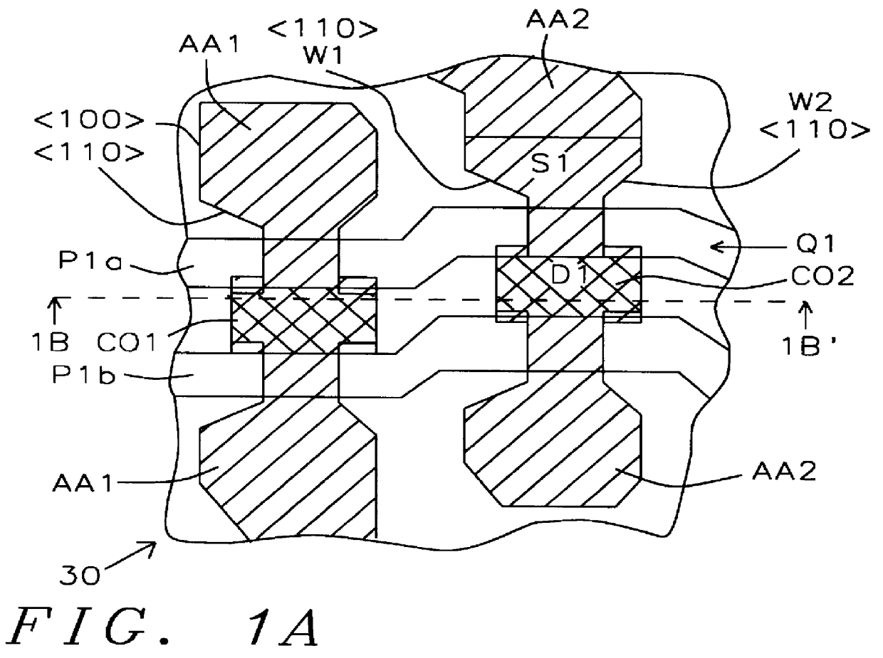
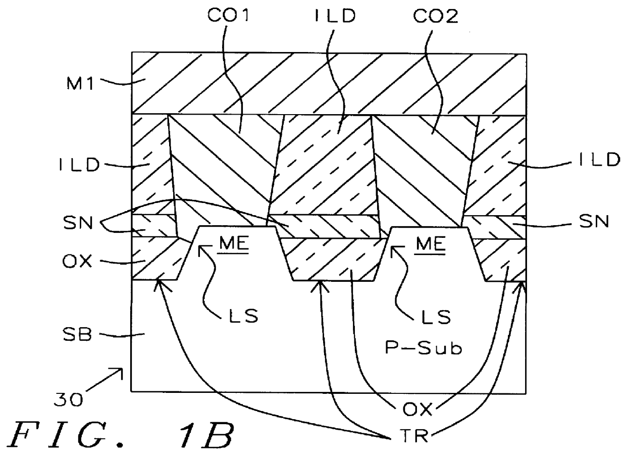
FIG. 1A shows a plan view of a portion of a first design considered for use as an SRAM design layout which has been found to have a problem of leakage paths. FIG. 1B shows a sectional, elevational view taken along line 1B-1B' in FIG. 1A. The device 30 which includes an SRAM is formed on a P- doped silicon substrate SB.

Referring to FIG. 1A the device 30 includes two vertically extending active areas AA1 / AA2, two horizontally extending word lines P1a and P1b composed of a conventional polysilicon 1 metallization layer. Word lines P1a and P1b include the gate electrodes of pass gate transistors Q1 and Q2 in FIG. 3. The contacts CO1 and CO2 are located between the word lines P1a and P1b extending down to active areas AA1 / AA2 respectively. Source region S1 and drain region D1 (formed in P- doped silicon substrate SB) are shown above and below the word line P1a in FIG. 1A in the active area AA2. The drain region D1 is square and the source region S1 is smaller and ...


PUM


Abstract

An SRAM device has STI regions separated by mesas and doped regions including source / drain regions, active areas, wordline conductors and contacts in a semiconductor substrate is made with a source region has 90 DEG transitions in critical locations. Form a dielectric layer above the active areas. Form the wordline conductors above the active areas transverse to the active areas. The source and drain regions of a pass gate transistor are on the opposite sides of a wordline conductor. Form the sidewalls along the <100> crystal plane. Form the contacts extending down through to the dielectric layer to the mesas. Substrate stress is reduced because the large active area region formed in the substrate assures that the contacts are formed on the <100> surfaces of the mesas are in contact with the mesas formed on the substrate and that the <110> surfaces of the silicon of the mesas are shielded from the contacts.

Description

1. Field of the InventionThis invention relates to semiconductor memory devices and more particularly to the configuration of SRAM memory devices.2. Description of Related ArtMechanical stress has been a problem which has existed in Shallow Trench Isolation (STI) technology. Mechanical stress tends to induce crystal defects which will result in creating leakage paths. It is necessary that such leakage paths should be suppressed to improve yield.In U.S. Pat. No. 5,466,632 of Lur et al. a FOX region with curvilinear boundaries is employed to reduce stress.In accordance with this invention, 90 degree transitions are employed at critical locations, while using 45 degree transition as few times as possible, where STI technology is used in an SRAM layout.Problems which are solved by the present invention are as follows:1. Leakage is decreased by reduction of crystal defects.2. Large contact (CO) / active area (AA) extension reduces the difficulties associated with photolithographic misalign...

Claims


Application Information

Patent Timeline
Patent Type & Authority Patents(United States)
IPC IPC(8): H01L27/11
CPCH01L27/1112Y10S257/903H10B10/15
Inventor WUU, SHOU-GWOLEE, JIN-YUANYAUNG, DUN-NIANLEE, JENG-HAN
Owner TAIWAN SEMICON MFG CO LTD
Why Eureka
Try Eureka