

Wafer inspection system for distinguishing pits and particles
a technology of inspection system and filter, applied in the direction of optical radiation measurement, semiconductor/solid-state device testing/measurement, instruments, etc., can solve the problem of wasting time and resources
- Summary
- Abstract
- Description
- Claims
- Application Information
AI Technical Summary
Benefits of technology
Problems solved by technology
Method used
Image

Examples
Embodiment Construction
The present invention will be described more fully hereinafter with reference to the accompanying drawings in which specific embodiments of the invention are shown. This invention may, however, be embodied in many different forms and should not be construed as limited to the illustrated embodiments set forth herein; rather, these illustrated embodiments are provided so that this disclosure will be thorough and complete and will fully convey the scope of the invention to those skilled in the art. Like numbers refer to like elements throughout.
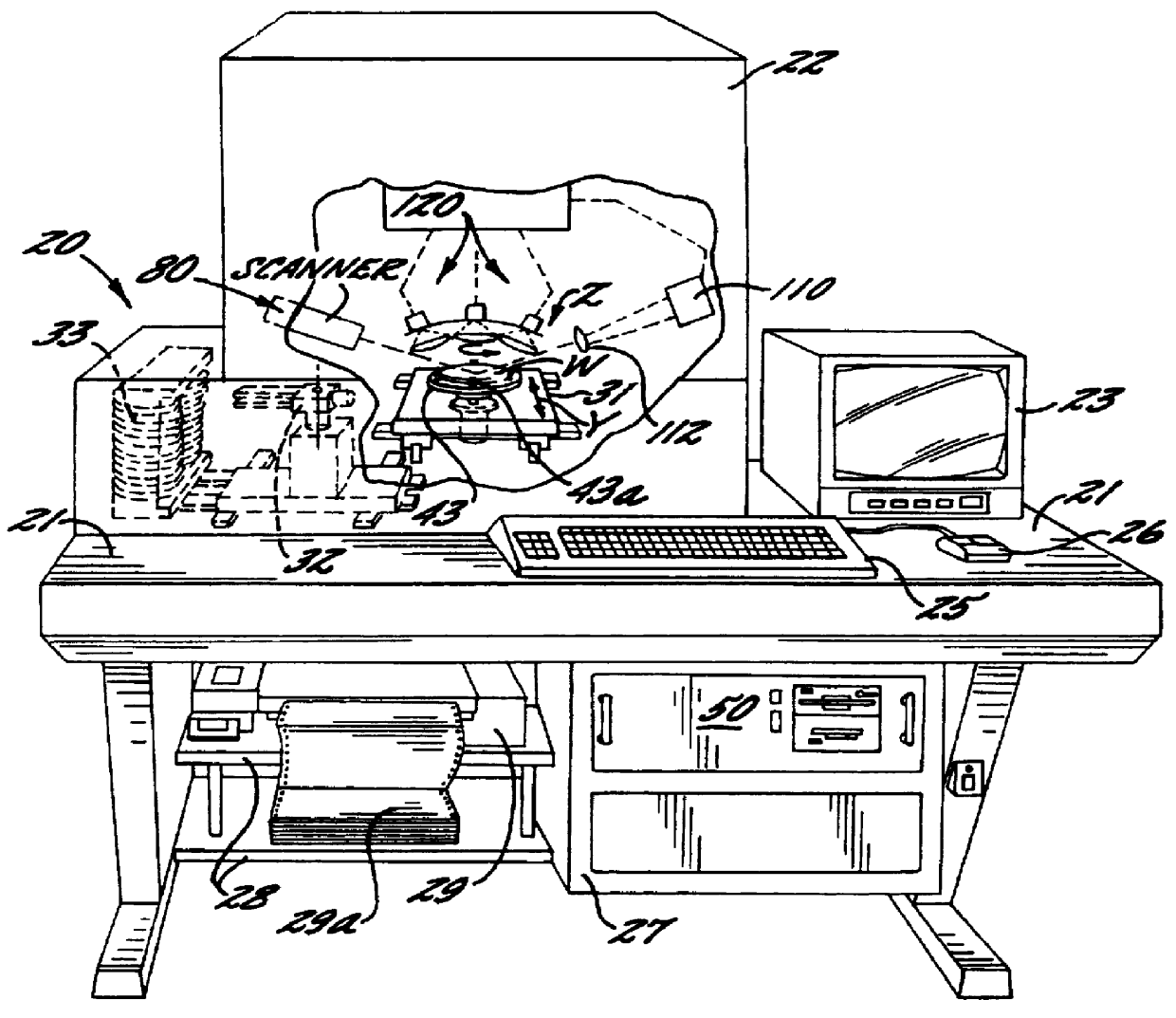
FIG. 1 is a perspective view of a surface inspection system 20 for detecting defects such as particles, pits and the like on a surface of a workpiece W or article, such as a silicon wafer. Portions of the system 20 are broken away for purposes of clarity and shown by phantom lines to illustrate various elements of the surface inspection system 20. The surface inspection system 20 is suitably used for inspecting the surface of unpatterned wafers ...
PUM
 Abstract
Description
Claims
Application Information