Electronic device and integrated circuit

a technology of integrated circuits and electronic devices, which is applied in the direction of semiconductor devices, radiation controlled devices, semiconductor/solid-state device details, etc., can solve the problems of contact failure, failure of contact, and failure of circuit hammering

Inactive Publication Date: 2000-09-19
SEMICON ENERGY LAB CO LTD
View PDF4 Cites 22 Cited by
  • Summary
  • Abstract
  • Description
  • Claims
  • Application Information

AI Technical Summary

Problems solved by technology

That is, this region is not utilized for the contact and is a factor hampering the integration of the circuit.
There is also a problem when a design rule is made rigorous in order to increase the integration that the area of the contact is reduced in proportion to square thereof.
Such circumstance may cause a failure in the contact.
That is, it may cause heat locally in the contact, causing the failure of the contact.
The more rigorous the design rule is, the more serious this problem becomes.

Method used


Image

  • Electronic device and integrated circuit
  • Electronic device and integrated circuit
  • Electronic device and integrated circuit

Examples


first embodiment

[First Embodiment]

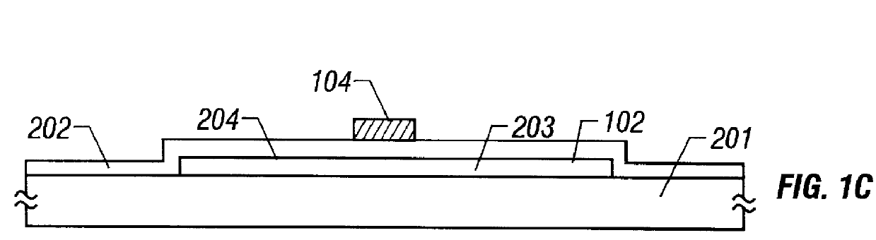
FIGS. 1 through 3 schematically show a process for fabricating an integrated circuit according to the present embodiment. A thin film transistor shown in the present embodiment has a form called a top gate type in which a gate electrode is positioned above an active layer.

At first, a glass substrate 201 is prepared as shown in FIG. 1B. Then, an underlying layer not shown is formed on the glass substrate 201. A silicon oxide film is used as the underlying layer.

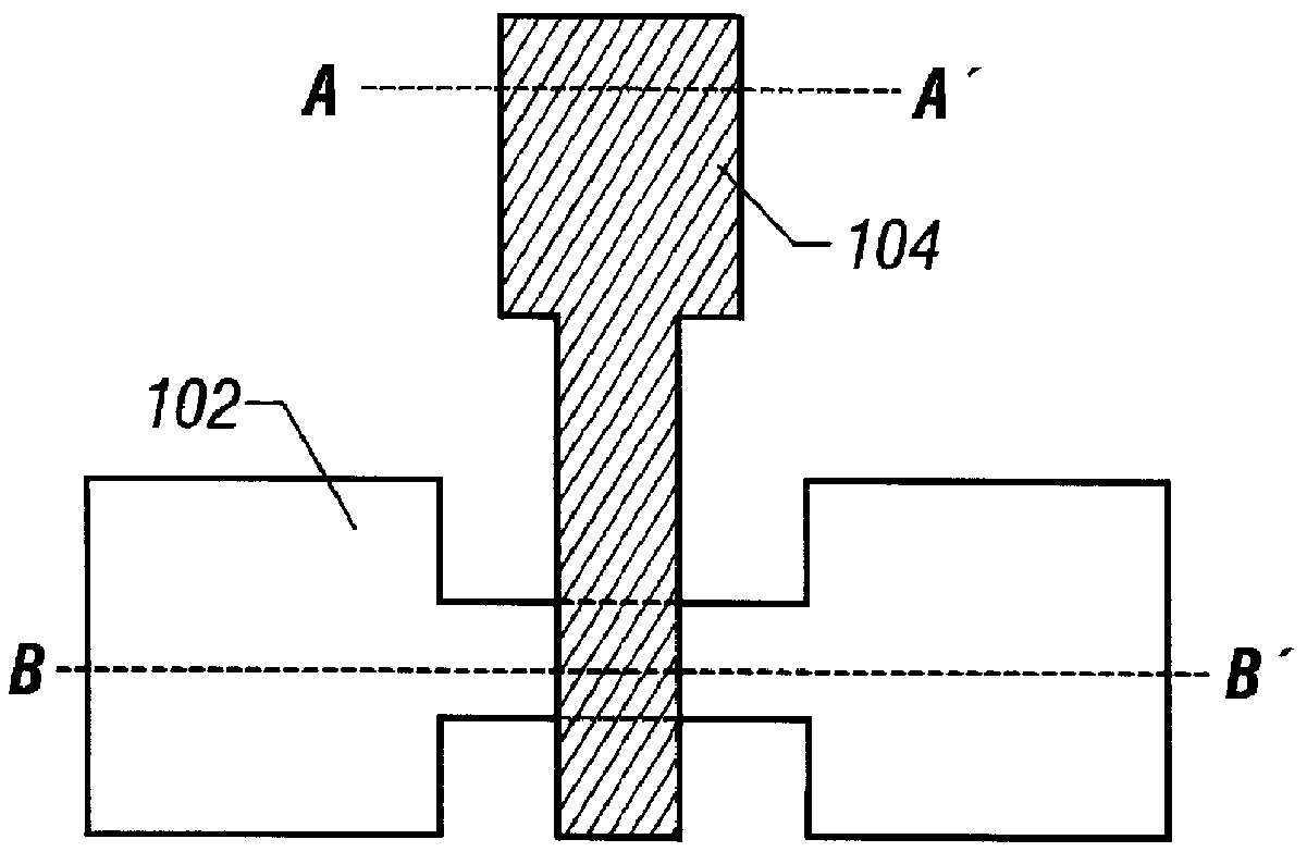
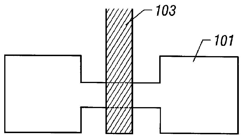
Next, an amorphous silicon film not shown is formed by means of plasma CVD or low pressure thermal CVD. Then, laser light is irradiated to the amorphous silicon film thus obtained to obtain a crystal silicon film. This crystal silicon film is patterned further to obtain active layers 101 and 102 shown in FIG. 1A.

After obtaining the active layers 101 and 102 of the thin film transistors, a gate insulating film 202 shown in FIG. 1B is formed. A silicon oxide film is used for the gate insulating film 202.

After f...

second embodiment

[Second Embodiment]

The invention disclosed in the present specification may be utilized in an active matrix liquid crystal display in which peripheral driving circuits are integrated.

It is very useful to utilize the invention disclosed in the present specification in the active matrix liquid crystal display in which peripheral driving circuits are integrated because the peripheral driving circuits are required to be highly integrated.

FIG. 7A shows an equipment called a digital still camera, an electronic camera or a video movie which is capable of displaying motion pictures.

This equipment has functions of electronically preserving images taken by a CCD camera (or appropriate photographing means) disposed at a camera section 2002 and of displaying the images on a liquid crystal display 2003 disposed on a main body 2001. The equipment may be controlled by manipulating control buttons 2004. The invention disclosed in the present specification is applied to a peripheral driving circuit ...

third embodiment

[Third Embodiment]

The present embodiment is a case when the invention disclosed in the present specification is applied to an integrated circuit composed of bottom gate type thin film transistors.

FIG. 8A is a plan view of the thin film transistors of the present embodiment. FIG. 8B is a section view taken along a line C-C' in FIG. 8A and FIG. 8C is a section view taken along a line D-D' in FIG. 8A.

In the present embodiment, gate electrodes 801 and 802 are formed on a substrate 901 at first. The gate electrodes 801 and 802 are formed by molybdenum silicide in the present embodiment.

Next, a silicon oxide film which functions as a gate insulating film 902 is formed. Then, active layers 803 and 804 made of crystal silicon film are formed thereon.

Next, although not shown, source and drain regions are formed by selectively implanting impurity ions to the active layers 803 and 804. After implanting the impurity ions, the source and drain regions are activated by irradiating laser light.

Nex...


PUM


Abstract

The present invention provides an integrated circuit structure in which an area necessary for making contact is assured in a multi-layered wiring structure even when a design rule is made rigorous. In a structure in which wires separated above and below by an interlayer insulating film are contacted, the wire at the lower layer is patterned into a pattern of the wire at the upper layer which are made to contact. Thereby, the present invention allows the area necessary for making the contact to be largely assured and to deal with the micronization.

Description

1. Field of the InventionThe present invention disclosed in the present specification relates to a structure of a contact in a semiconductor integrated circuit having a multi-layered wiring structure.2. Description of Related ArtHitherto, there has been known a structure of an integrated circuit in which thin film transistors are integrated and arranged on a glass substrate or a quartz substrate.The thin film transistors are utilized mainly in an active matrix type liquid crystal display. The active matrix liquid crystal display has a structure in which the thin film transistor is disposed in each of pixels arranged in a matrix of several hundreds x several hundreds pixels. The thin film transistor disposed in each pixel has a function of individually controlling charge input / output to / from a pixel electrode.There has been also known a structure in which peripheral driving circuits for driving the active matrix region are constructed by the thin film transistors and are integrated o...

Claims


Application Information

Patent Timeline
Patent Type & Authority Patents(United States)
IPC IPC(8): H01L27/12H01L21/768H01L21/3213H01L29/786
CPCH01L27/12H01L21/76
Inventor YAMAZAKI, SHUNPEIKOYAMA, JUNTERAMOTO, SATOSHI
Owner SEMICON ENERGY LAB CO LTD
Why Eureka
Try Eureka