
Photomask used in fabrication of mask read only memory

a technology of read only memory and photomask, which is applied in the field of semiconductor device fabrication, can solve the problems of poor adhesion ability, weak light interference effect, and pattern resolution that cannot be further enhanced

Inactive Publication Date: 2000-10-31
UNITED MICROELECTRONICS CORP
View PDF1 Cites 3 Cited by
  • Summary
  • Abstract
  • Description
  • Claims
  • Application Information

AI Technical Summary

Problems solved by technology

The desired pattern of the photomask is transferred onto a semiconductor substrate through a light source so that it has an intrinsic issue of a pattern resolution.
Particularly, when device dimension goes down to 0.25 microns or smaller, the light interference effect is stronger, and the pattern resolution cannot be further enhanced.
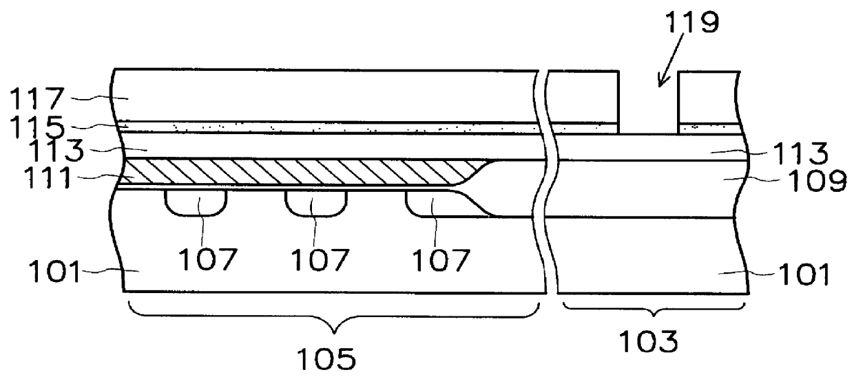
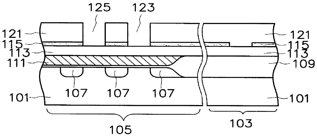
This is because the bonding pad usually is made of aluminum, which has poor adhesion capability with the titanium nitride of the barrier layer 115.
The fabrication cost and the fabrication efficiency are still not the most economical.

Method used


Image

  • Photomask used in fabrication of mask read only memory
  • Photomask used in fabrication of mask read only memory
  • Photomask used in fabrication of mask read only memory

Examples


Embodiment Construction

The invention introduces a photomask that includes a code area opening pattern and a bonding pad opening pattern combined together so that the bonding pads and code areas are simultaneously formed. Moreover, since the bonding pads and code areas can be simultaneously formed, there is no transition time between the bonding pad being formed beforehand and the code areas being actually formed later.

FIG. 3A is a top view of a photomask, schematically illustrating an opening pattern layout, according to a preferred embodiment of the invention. FIG. 3B is a cross-sectional view of a portion of a photomask, schematically illustrating a pattern layout of the photomask, according to a preferred embodiment of the invention.

In FIG. 3A, a photomask 350 includes a code area pattern region 352, which usually is at the central part of the photomask 350 and includes several code area openings 356. A bonding pad pattern region 354 including several bonding pad pattern openings 358 usually surroundin...


PUM


Abstract

A photomask used in a formation of a mask read only memory (mask ROM) device is provided. The photomask contains a bonding pad opening pattern and a code area opening pattern so that bonding pads and code areas are simultaneously formed in a more economical operation.

Description

1. Field of the InventionThis invention relates to semiconductor fabrication, and more particularly to a photomask used in fabrication of a mask read only memory (ROM) device.2. Description of Related ArtA memory device is widely used in the information industry, and is particularly used in microprocessors and computers. In order to achieve a faster speed of information exchange with more tremendous quantity in a more convenient way, the information products need the properties of small dimensions and reduced weight. The properties are necessarily met by a memory with higher memory capacity and faster access speed. Currently, a mask ROM with embedded bit lines is a common memory structure because it can be fabricated with very high integration.The fabrication of a memory device includes not only forming a memory cell and encoding but also forming bonding pads. The fabrication processes for encoding and forming bonding pads also include photomasks with proper patterns.A phototmask ty...

Claims


Application Information

Patent Timeline
IPC IPC(8): G03F1/08H01L21/70H01L21/8246G03F1/14G03F1/00G03F1/42G03F1/46
CPCG03F1/42H01L27/11293H01L27/1126G03F1/46G03F1/14G03F1/26H10B20/65H10B20/383
Inventor CHEN, G. L.TSENG, JACK
Owner UNITED MICROELECTRONICS CORP
Learn More