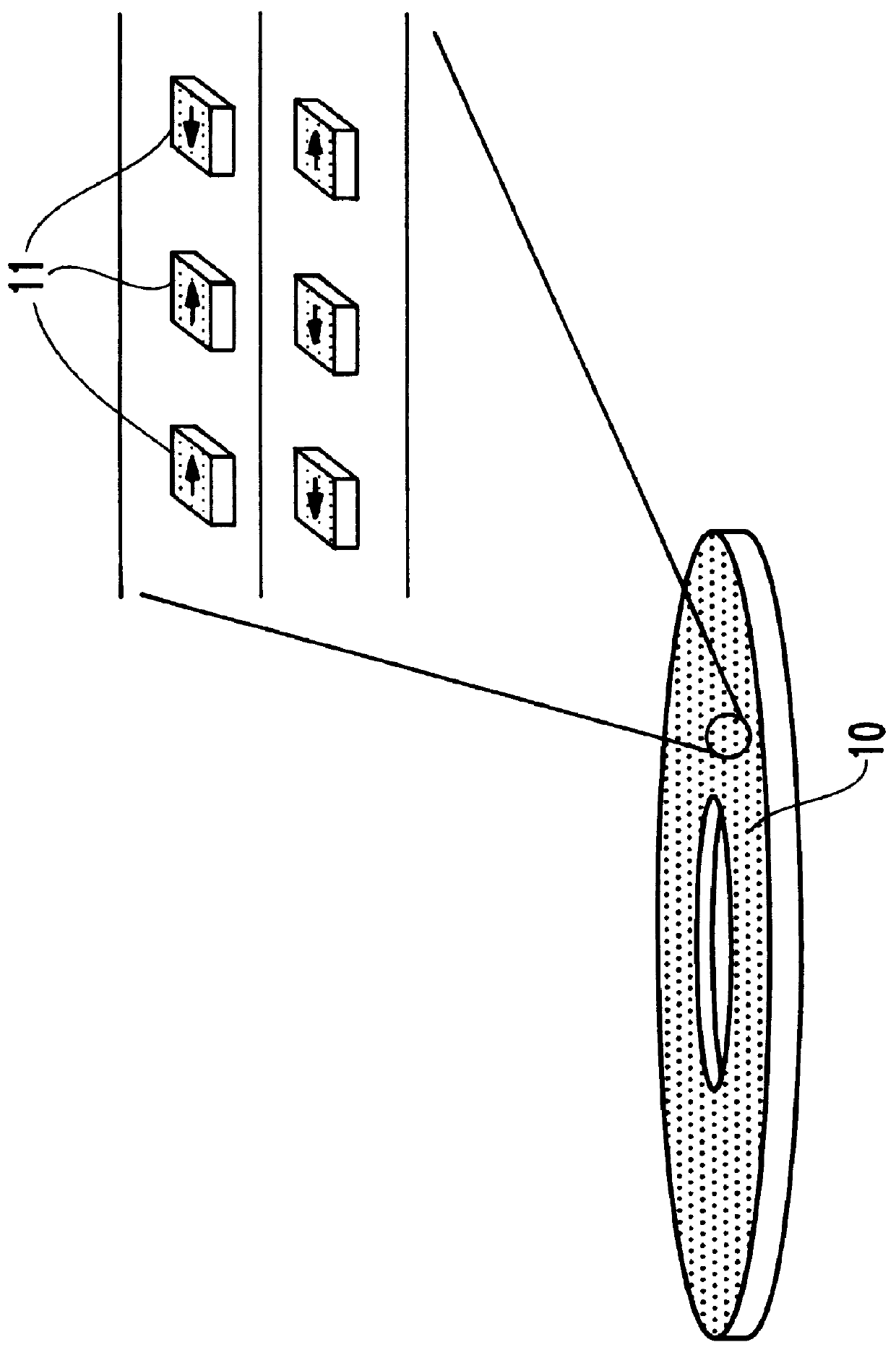
High density magnetic recording medium utilizing selective growth of ferromagnetic material
a high density, magnetic recording medium technology, applied in the field of magnetic recording medium, can solve the problems of loss of written data, loss of recording density, loss of density in the media required
- Summary
- Abstract
- Description
- Claims
- Application Information
AI Technical Summary
Problems solved by technology
Method used
Image

Examples
first embodiment (
Using Ti evaporation:)
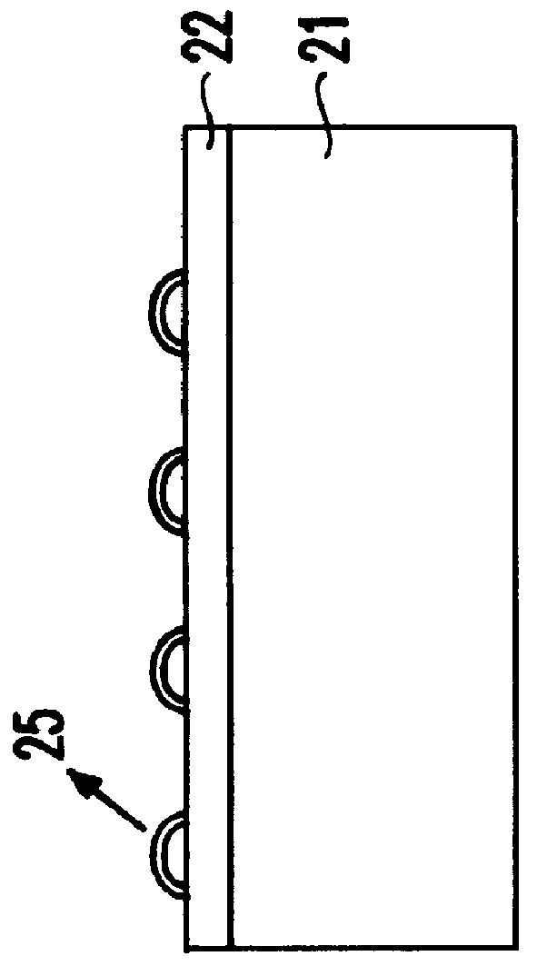
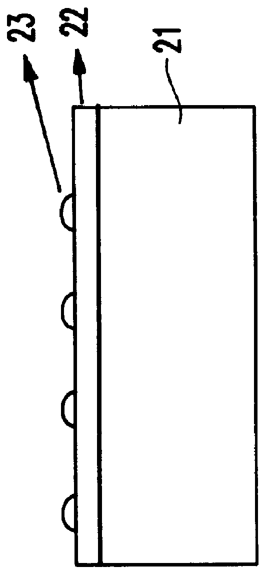
In a first embodiment, as shown in FIGS. 2(a)-2(d), a substrate 21 such as a silicon wafer 20 is provided having a thickness within a range of about 100 .mu.m to about 10000 .mu.m. The substrate is not limited to silicon wafers, but could be a polymeric media, a metal, or the like. The choice of silicon is made only for convenience of explanation.
As shown in FIG. 2(a), the Si surface is coated with a thin layer of SiO.sub.2 having a thickness greater than about 100 nm in thickness. If the thickness is below 100 nm, as long as a continuous film is formed on the substrate, it is sufficient.
Thereafter, as shown in FIG. 2(b), the wafer 20 is inserted into a vacuum chamber equipped with a Ti evaporation source which is quite commonly known in the art. A small amount of Ti (e.g., equivalent to 1-2 monolayers of Ti deposition, a commonly recognized thickness) is performed on the Si wafer in the vacuum chamber. Since only a very small amount of Ti is delivered, the Ti ...
second embodiment (
Using porous Si)
The technique for making nanostructured films using porous silicon, according to the second embodiment of the present invention, is shown in the cross-sectional view of FIGS. 3(a)-3(d).
First, as shown in FIG. 3(a), a conducting silicon wafer 30 is provided having a conducting substrate 31, and a relatively thin Ti film 32 having a thickness substantially within a range of about 10 nm to about 1000 nm, and more preferably about 50 nm, is vacuum-deposited on top of the conducting substrate 31. The Ti film's thickness should be large enough, so that a uniform, continuous layer is formed, rather than islands (e.g., discontinuous areas) as described above in the first embodiment. The Ti 32 may be deposited either by using a thermal evaporation source for the Ti or a sputtering source. On top of the Ti layer 32, a silicon layer 33, preferably having a thickness within a range of about 20 nm to 1000 nm, and most preferably about 500 nm thick, is deposited again using a stan...
second embodiment
The second embodiment described above is preferred since it allows for exact definition of the size and shape of the CrO.sub.2 elements at predetermined locations. However, a drawback is that the second embodiment involves additional processing steps as compared to the first embodiment.
PUM
| Property | Measurement | Unit |
|---|---|---|
| Fraction | aaaaa | aaaaa |
| Thickness | aaaaa | aaaaa |
| Thickness | aaaaa | aaaaa |
Abstract
Description
Claims
Application Information
 - R&D Engineer
- R&D Manager
- IP Professional
- Industry Leading Data Capabilities
- Powerful AI technology
- Patent DNA Extraction
Browse by: Latest US Patents, China's latest patents, Technical Efficacy Thesaurus, Application Domain, Technology Topic.
© 2024 PatSnap. All rights reserved.Legal|Privacy policy|Modern Slavery Act Transparency Statement|Sitemap