Method for increasing capacitance

a capacitance electrode and capacitance technology, applied in the direction of capacitors, electrical equipment, semiconductor devices, etc., can solve the problems of inability to achieve appreciably larger capacitance electrodes than conventional polysilicon, and inability to achieve further improvement of capacitan

Inactive Publication Date: 2000-11-28
AISAWA TECH
View PDF3 Cites 10 Cited by
  • Summary
  • Abstract
  • Description
  • Claims
  • Application Information

AI Technical Summary

Problems solved by technology

Further reductions in capacitance would require more frequent refresh operations for the DRAM, which are undesirable because at least portions of the DRAM are unavailable for the reading and writing of information during refresh operations.
Substrate deposition temperatures of ten degrees higher or lower than 590.degree. C. produced an unacceptable surface texture, that is, these conditions produced an undesirably flat surface which did not provide appreciab

Method used


Image

  • Method for increasing capacitance
  • Method for increasing capacitance
  • Method for increasing capacitance

Examples


Embodiment Construction

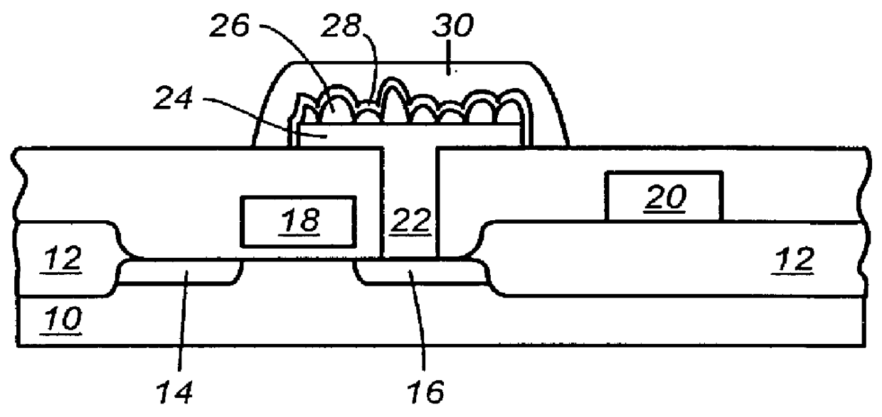
It is accordingly an object of this invention to provide an increased capacitance utilizing an HSG-Si layer in the process of making an electrode.

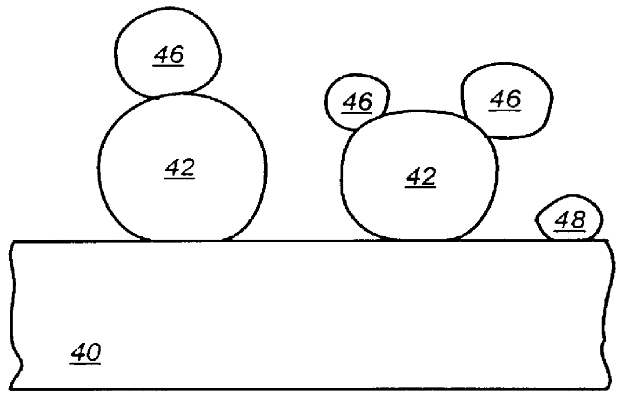
A first aspect of the present invention forms a semiconductor device by providing a layer of silicon on or above a silicon substrate and providing a first layer of hemispherical-grained silicon on the layer of silicon. A second layer of hemispherical-grained silicon is deposited over the first layer of hemispherical-grained silicon so that independent grains of hemispherical-grained silicon are formed on the grains of the first layer of hemispherical-grained silicon.

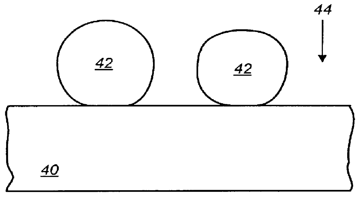
Another aspect of the present invention forms a semiconductor device by providing a deposition substrate comprising silicon and depositing a first layer of hemispherical-grained silicon over the deposition substrate in a first deposition process. A second layer of hemispherical-grained silicon is deposited over the deposition substrate in a second deposition process so that gra...


PUM


Abstract

The capacitor of a DRAM cell is formed by depositing a layer of doped polysilicon, patterning the layer of doped polysilicon to define the extent of the capacitor's lower electrode and then depositing a first layer of hemispherical-grained silicon (HSG-Si) on the layer of doped polysilicon. Growth of the first layer of HSG-Si is interrupted and then a second layer of HSG-Si is grown. In one aspect, growth of the first layer of HSG-Si may be interrupted by either cooling the deposition substrate or stopping deposition for a period of time and then reinitiating deposition to provide a second layer of HSG-SI on the surface of the electrode. The interruption of the growth of the first layer, whether by cooling or by delay, is sufficient if the reinitiated growth initiates in a manner that is independent of the first process; i.e., the second layer of HSG-Si grows independently. In a different aspect of the invention, growth of the first layer may be interrupted by removing the electrode from the deposition system and performing an etch back operation. After the etch back operation, the electrode is reintroduced to the deposition system and a second layer of HSG-Si is grown on the etched surface. This textured silicon structure forms the lower electrode of the DRAM capacitor.

Description

1. Field of the InventionThe present invention relates to the formation of high capacitance structures in integrated circuit devices and, more particularly, to the formation of electrodes which incorporate at least one textured surface.2. Description of the Related ArtHistorically, increasing the density of integrated circuit devices has been accomplished in part by decreasing the size of structures such as wiring lines and transistor gates and by decreasing the separation between the structures which make up the integrated circuit device. Reducing the size of circuit structures is generally referred to as decreasing the "design rules" used for the manufacture of the integrated circuit device. For dynamic random access memories (DRAMs), information is typically stored by selectively charging or discharging each capacitor of an array of capacitors formed on the surface of a semiconductor substrate. Most often, a single bit of binary information is stored at each capacitor by associat...

Claims


Application Information

Patent Timeline
IPC IPC(8): H01L21/02H01L21/8242H01L21/70
CPCH01L28/84H01L27/1085H10B12/03
Inventor YEW, TRI-RUNGLUR, WATERSUN, SHIH-WEI
Owner AISAWA TECH
Why Eureka
Try Eureka