Analog to digital converter using several cascade-connected interpolation circuits
- Summary
- Abstract
- Description
- Claims
- Application Information
AI Technical Summary
Problems solved by technology
Method used
Image
Examples
Embodiment Construction
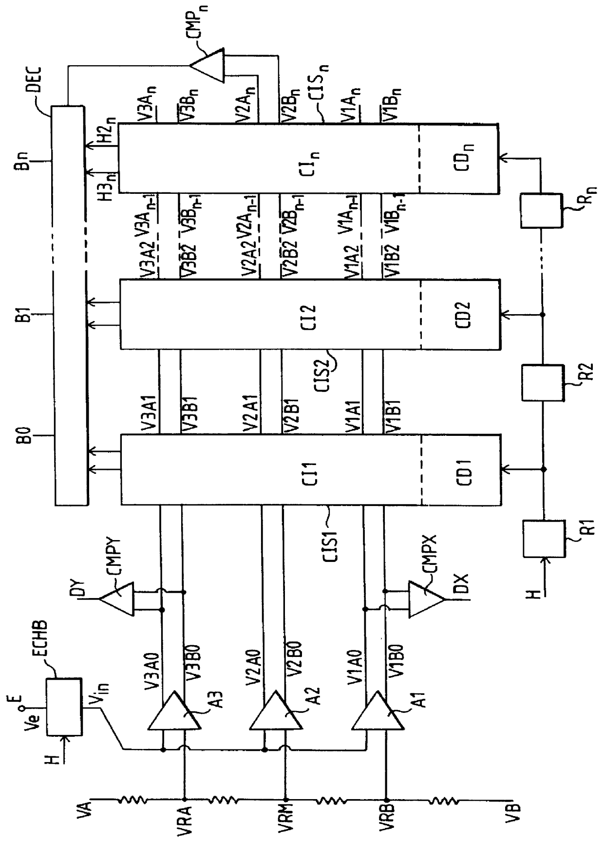
The general structure of the converter according to the invention is shown in FIG. 1.
The function of this converter is to give an n-bit digital signal representing, in digital form, the value of the amplitude of an input analog signal Vin. The m bits, according to a binary code, represent a value of Vin out of 2.sup.n values evenly distributed between two main reference values VRA and VRB.
The input signal Vin may take any values between two extreme values Vext1 and Vext2 which may go well beyond the range of values located between VRA and VRB but, in any case, the output of the converter gives a digital representation of Vin only if Vin is between VRA and VRB. It will be seen however that the converter can also give an upward overflow signal or a downward overflow signal indicating that Vin is beyond the range VRA to VRB.
The main reference voltages VRA and VRB as well as another main reference voltage VRM that is equidistant from the values VRA and VRB are each applied respectively ...
PUM
 Abstract
Description
Claims
Application Information


