Composite laminate circuit structure and method of forming the same

Inactive Publication Date: 2001-01-16
GLOBALFOUNDRIES INC
View PDF36 Cites 166 Cited by
  • Summary
  • Abstract
  • Description
  • Claims
  • Application Information

AI Technical Summary

Problems solved by technology

This requires precession drilling to form the plated through holes all of which is time consuming, especially where there is a large number of drilled holes required to form plated through holes.

Method used


Image

  • Composite laminate circuit structure and method of forming the same
  • Composite laminate circuit structure and method of forming the same
  • Composite laminate circuit structure and method of forming the same

Examples


Embodiment Construction

)

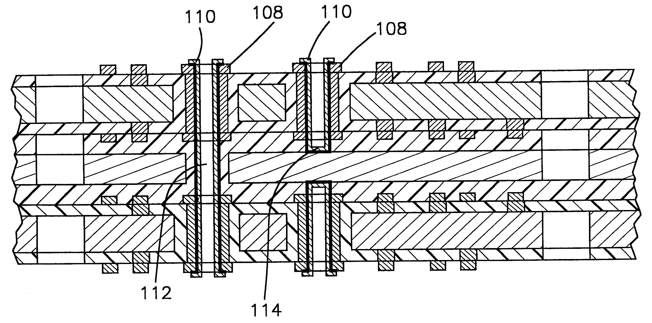
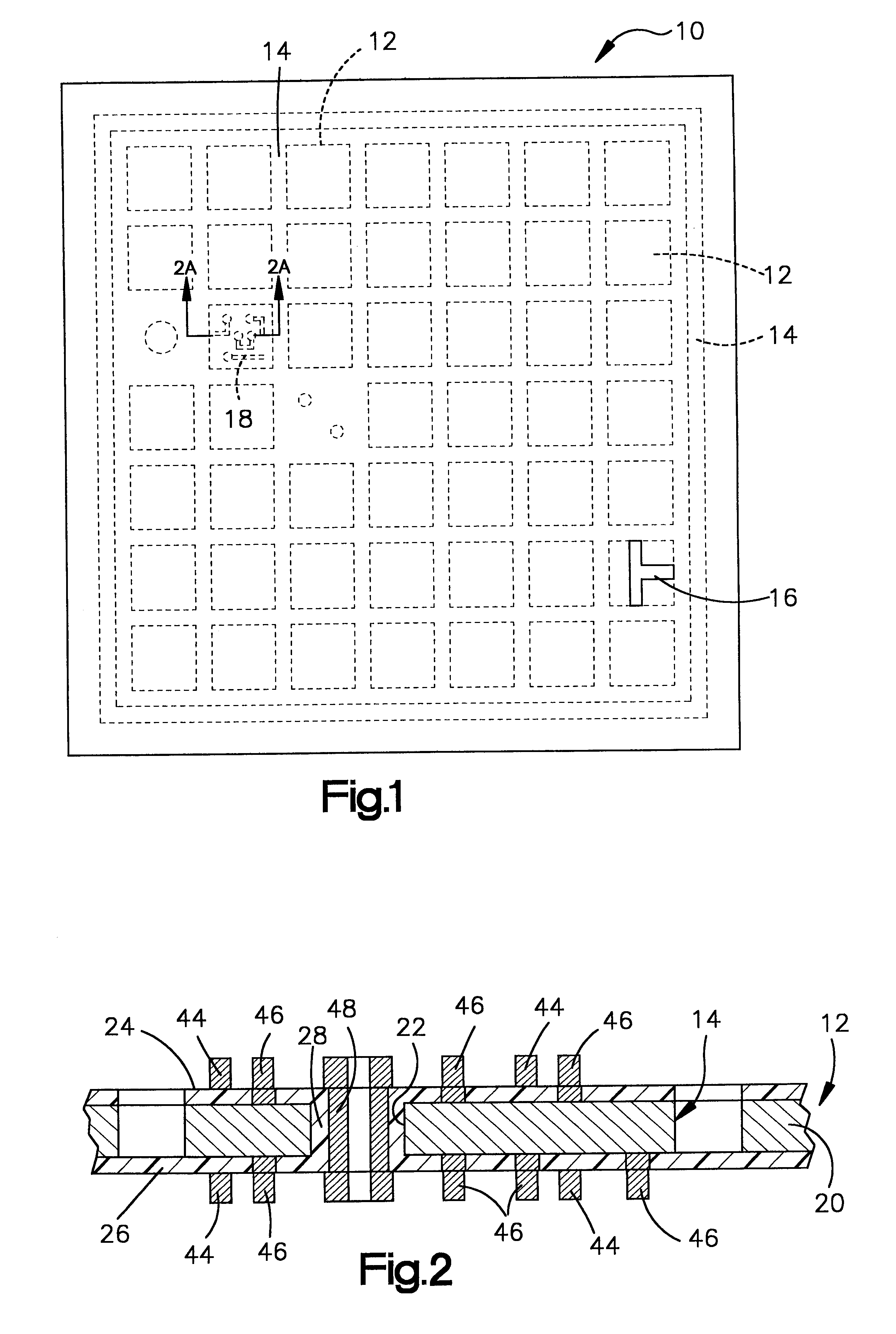
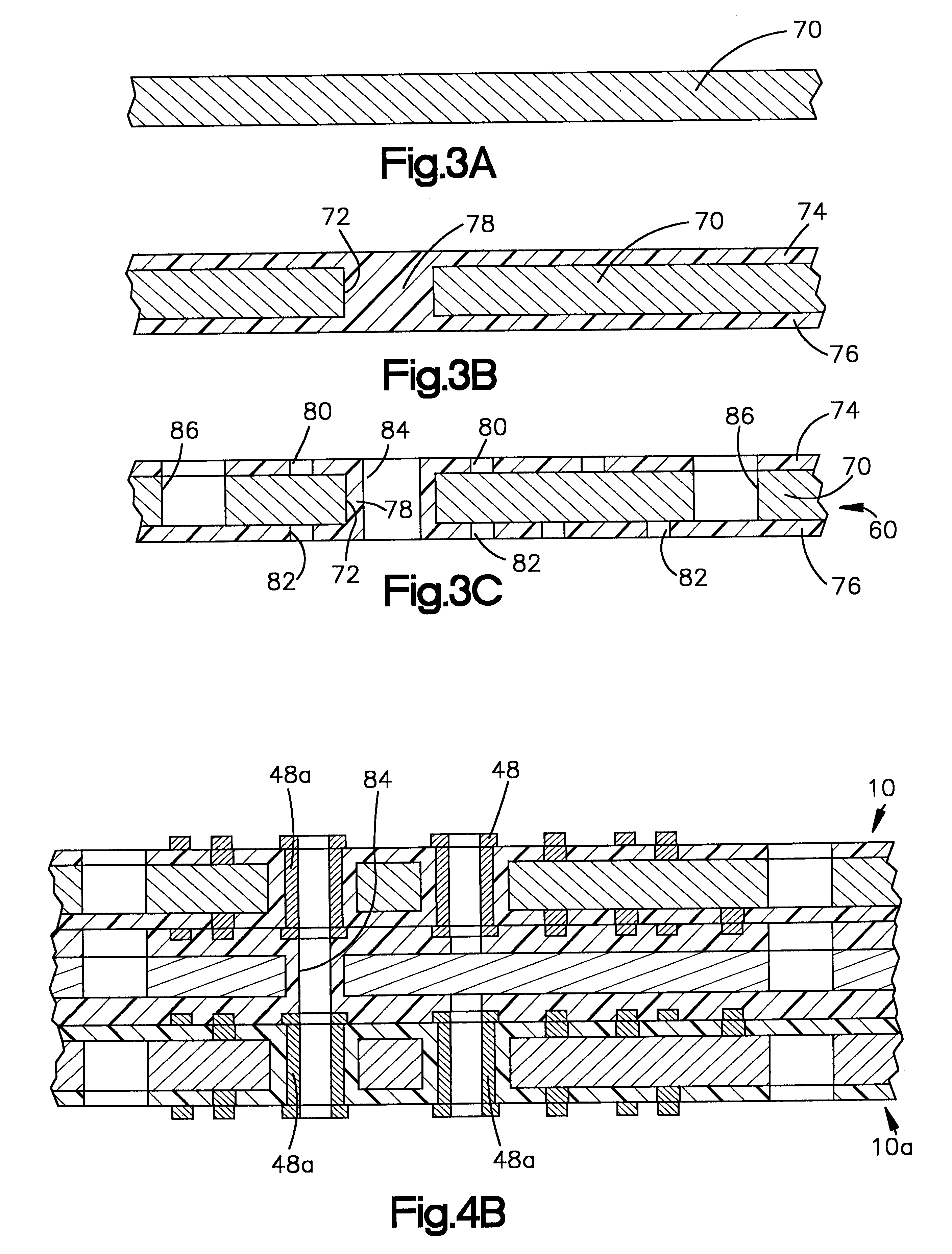
The present invention provides a technique and resulting structure wherein two or more essentially fully circuitized components can be joined together using one or more power plane components which power plane components are not circuitized when joined, but which are circuitized after joining with the circuitized components, to form a composite laminate structure of multiple levels of voltage planes and signal planes in which the circuitization of the signal plane components is essentially completed before the lamination of the components to form the final structure.

The invention will be described in its preferred embodiment, utilizing components formed according to the teachings of application Ser. No. 09 / 203,956; filed Dec. 2, 1998; entitled "Two Signal One Power Plane Circuit Board", and which is incorporated herein by reference. It is to be understood, however, that other circuitized components such as those formed according to the teachings of application Ser. No. 09 / 203,978; ...


PUM


Abstract

A method forming a composite laminate structure includes providing first and second circuit board element each having circuitry on at least one face thereof and plated through holes. A voltage plane element is provided having at least one voltage plane having opposite faces with layers of partially cured photodielectric material on each face. At least one hole is photopatterned and etched through the voltage plane element but completely isolated from the voltage plane. Each through hole in the voltage plane element is aligned with a plated through hole in each of the circuit board elements to provide a surface on the voltage plane element communicating with the plated through holes. The voltage plane is laminated between the circuit board elements and the photoimageable material on the voltage plane is fully cured. The surfaces of the voltage plane element communicating with the plated through holes in the circuit board elements are plated with a conducting material to establish a connection between the circuitry on the first and second circuit board elements.

Description

1. Field of the InventionThis invention relates generally to the formation of laminate circuit structures by photolithographic techniques, and more particularly to a method of forming composite laminate structures which utilizes a multiplicity of preformed circuits having signal and voltage planes and a laminate structure having a ground plane without signal planes.2. Background InformationA conventional technique of forming a laminate circuit board structures includes forming layers of dielectric material and electrically conducting material to provide multiple layers of circuits and voltage planes. Voltage planes can be either ground plane or power plane, and are sometimes collectively referred to as power planes. In one prior art technique of forming such structure, layers of dielectric material and conducting material successively applied, i.e. the dielectric material is applied and then voltage planes are supplied thereon and if necessary through holes formed by the drilling or...

Claims


Application Information

Patent Timeline
Patent Type & Authority Patents(United States)
IPC IPC(8): H05K3/42H05K3/46H05K3/00
CPCH05K3/429H05K3/4623H05K3/4641H05K3/0023H05K2201/09509H05K2201/09536H05K2201/096H05K2201/09809H05K3/46
Inventor KEESLER, ROSS W.MARKOVICH, VOYA R.PAOLETTI, JIM P.PERRINO, MARYBETHWILSON, WILLIAM E.
Owner GLOBALFOUNDRIES INC
Why Eureka
Try Eureka