Method for shielding of electronics

a shielding box and electronic technology, applied in the field of shielding electronics, can solve the problems of occupying a large place on the assembly base of the shielding box, affecting the shielding effect, and being difficult to manipula

Inactive Publication Date: 2001-02-27
TELEFON AB LM ERICSSON (PUBL)
View PDF32 Cites 60 Cited by
  • Summary
  • Abstract
  • Description
  • Claims
  • Application Information

AI Technical Summary

Problems solved by technology

A disadvantage of the method above is that the shielding boxes can be displaced or placed askew during the automatic mounting of the box over the components, whereby the shielding box can come into contact with the components which are placed near to its inner side.
A disadvantage of screwed or clamped joints is that they can be complicated to manipulate and that they are expensive.
A disadvantage when shielding boxes are soldered to the assembly base is that the solder, with which the shielding boxes are fixed to the assembly base, can come into contact with a component situated near the inner side of the shielding box, whereby the component is shortcircuited with the solder.
A disadvantage is that the box thereby takes up a large place on the assembly base.
A disadvantage of this method is that it requi

Method used


Image

  • Method for shielding of electronics
  • Method for shielding of electronics
  • Method for shielding of electronics

Examples


Embodiment Construction

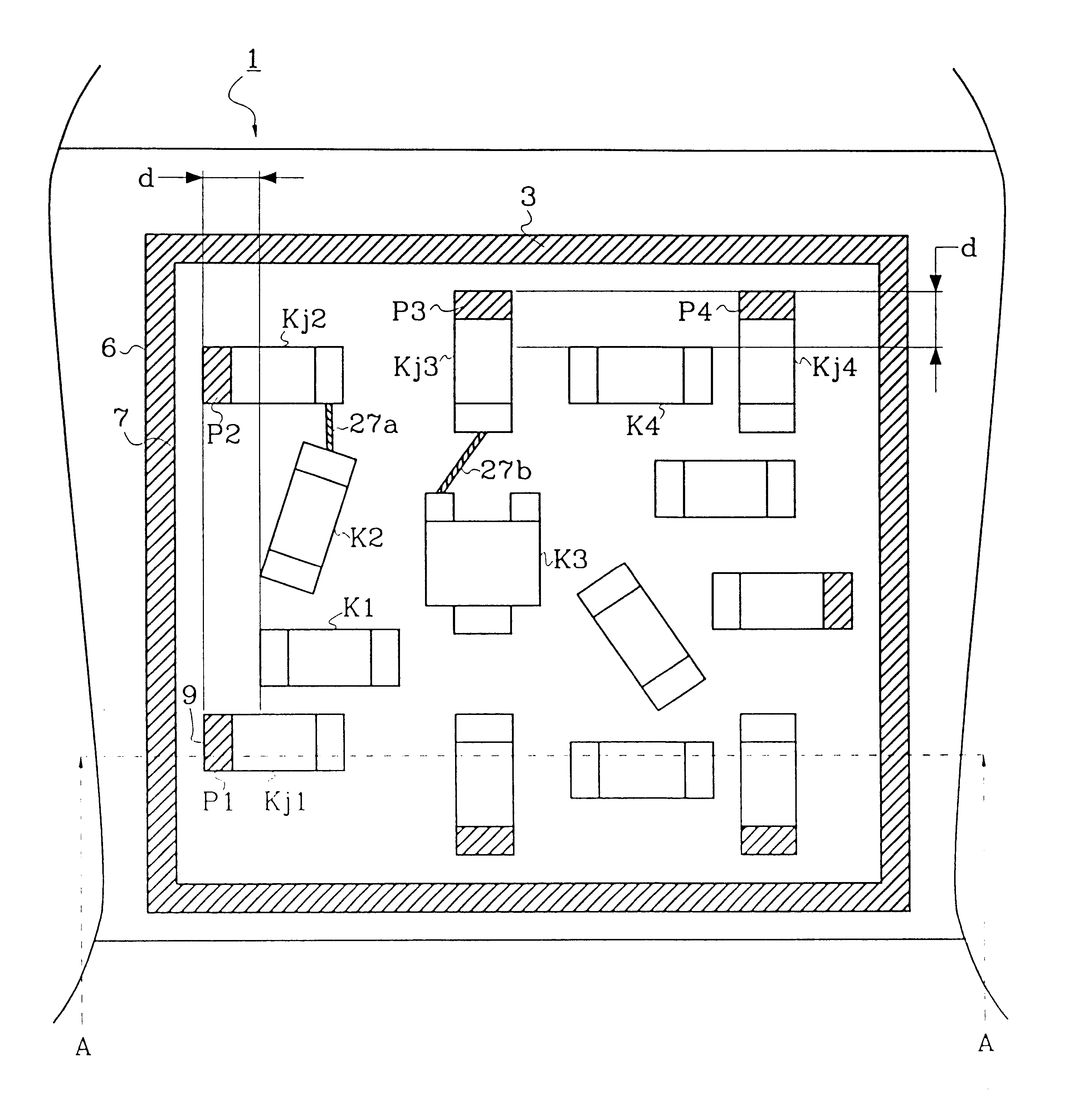
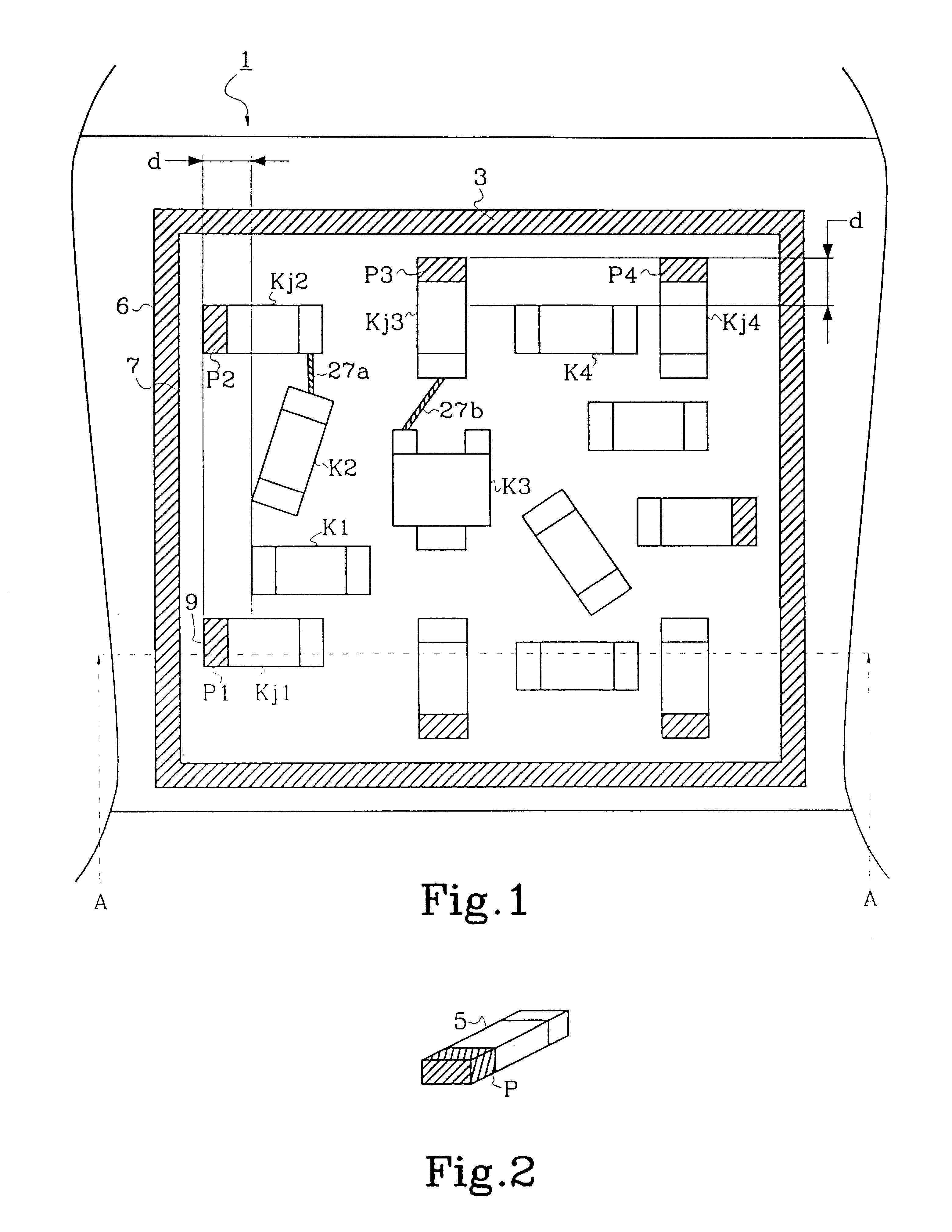
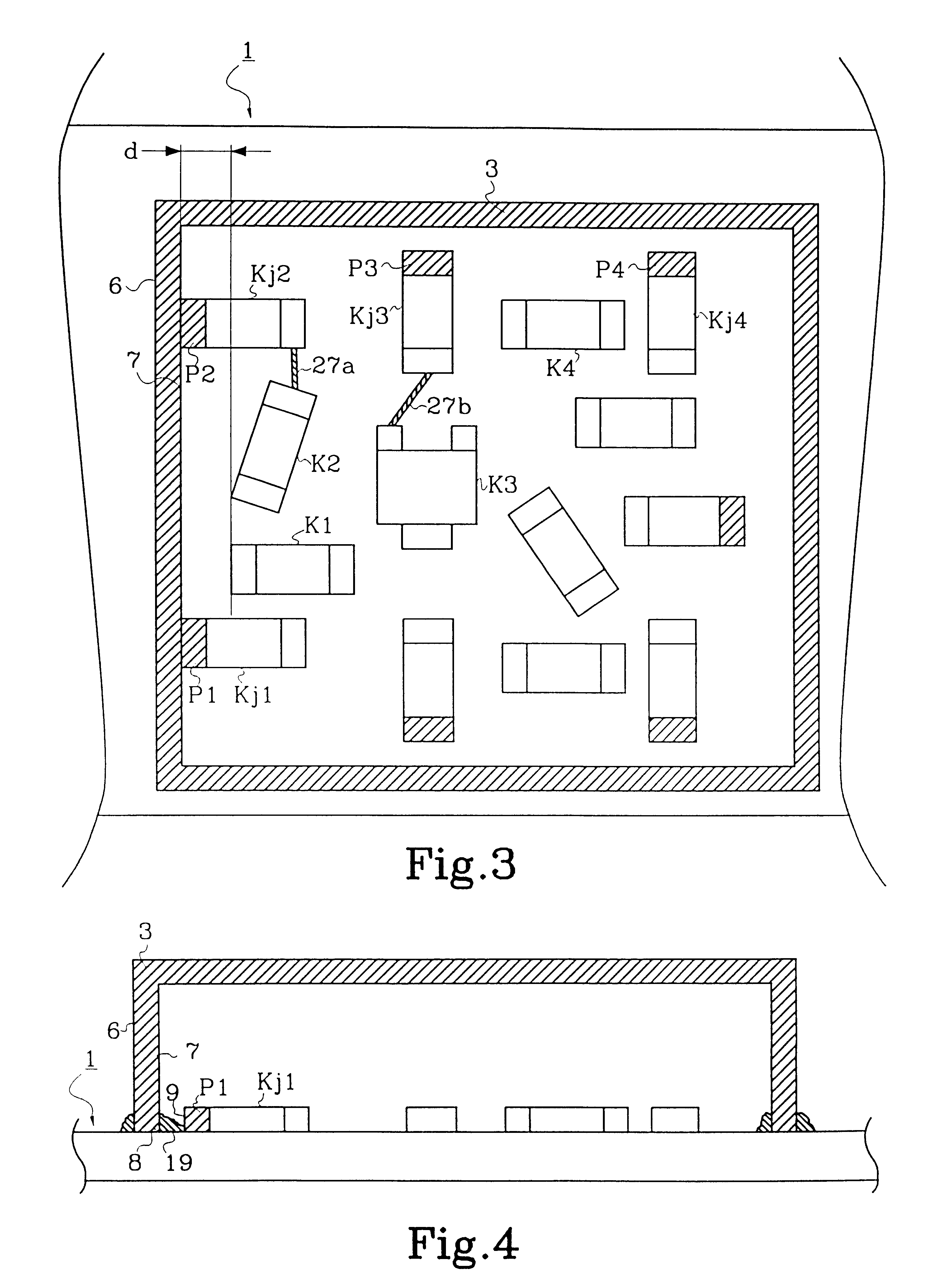
An example of an embodiment of the device according to the invention will be described below in relation to FIGS. 1 and 2, wherein a number of electronic components are desired to be shielded on an assembly base 1.

FIG. 1 shows a cross-section of a shielding unit in the shape of a rectangular box 3 with an outer and an inner rectangular contour. The base surface of the box is in contact with an assembly base 1, enclosing the shielded electronic components.

The figure also shows two strap conductors 27a, 27b which will be described in more detail below in connection with FIG. 5.

The assembly base 1 is, for example, a circuit board which carries the electronic components.

The shielding unit 3 comprises an outer side surface 6 and an inner side surface 7 with a bottom edge 8 which as well as its bottom base surface is in contact with the circuit board 1. The shielding unit 3 is manufactured in a suitable solderable metal.

The inner side surface 7 and the outer side surface 6 surround the sh...


PUM

PropertyMeasurementUnit
Distanceaaaaaaaaaa

Abstract

In a method for shielding electronics, a plurality of components to be shielded are arranged on a part of an assembly base to be shielded, each of the plurality of components having a first side including a first contact surface connectable to a common earth connection of the assembly base, each of the plurality of components further having a second contact surface, the plurality of components being arranged such that, for each of the plurality of components, the first side with the first contact surface faces out toward a periphery of the part of the assembly base. For each of the plurality of components, the first contact surface is connected to the earth connection. The plurality of components are shielded with a shielding device. For each of the plurality of components, the first contact surface is closer to the shielding device than the second contact surface.

Description

The present invention relates to an apparatus and a method for shielding electronic components on an assembly base.STATE OF THE ARTAccording to the prior art, electronic components, also called components, attached to an assembly base in e.g. radio receivers, television apparatuses, com-puters, transceivers (transmitters) and telephones in many cases need to be shielded from the environment in order to prevent undesirable radiation from the electronic compo-nents. Examples of such radiation can be radio frequency radiation, so-called RF-radiation (Radio Frequency radiation). Electronic components can also in certain cases be shielded in order to be protected against the influence of e.g. static electricity, so-called ESD (Electro Static Discharge).Examples of electronic components are resistors, capacitors, coils or transistors, and integrated circuits. The assembly base ban be printed circuit board.Such electronic components comprise two or more contact connections, so-called poles...

Claims


Application Information

Patent Timeline
IPC IPC(8): H05K9/00H05K1/02
CPCH05K1/0218H05K9/0024Y10T29/49144Y10T29/49146H05K9/0026H05K9/00
Inventor LARSSON, ANDERS
Owner TELEFON AB LM ERICSSON (PUBL)
Why Eureka
Try Eureka