Thermally enhanced quad flat non-lead package of semiconductor

a technology of semiconductor and non-lead package, which is applied in the direction of semiconductor/solid-state device details, semiconductor devices, electrical apparatus, etc., can solve the problems of affecting the performance of electronic devices, generating increases, and reducing the yield of products

Inactive Publication Date: 2001-03-06
SILICONWARE PRECISION IND CO LTD
View PDF7 Cites 374 Cited by
  • Summary
  • Abstract
  • Description
  • Claims
  • Application Information

AI Technical Summary

Problems solved by technology

However, because of the demand for diminishing the thickness of the package, this conventional package structure is apt to expose the bonding wire 114 while encapsulating, thereby, the yield of the product become lower.
Additionally, as the operating speed of the device of the integrated circuit becomes faster and faster nowadays. the heat generated increases accordingly, and since the conventional package structure is unable to provide a better way of heat dissipation, the performance of the electronic device will be affected.

Method used


Image

  • Thermally enhanced quad flat non-lead package of semiconductor
  • Thermally enhanced quad flat non-lead package of semiconductor
  • Thermally enhanced quad flat non-lead package of semiconductor

Examples


Embodiment Construction

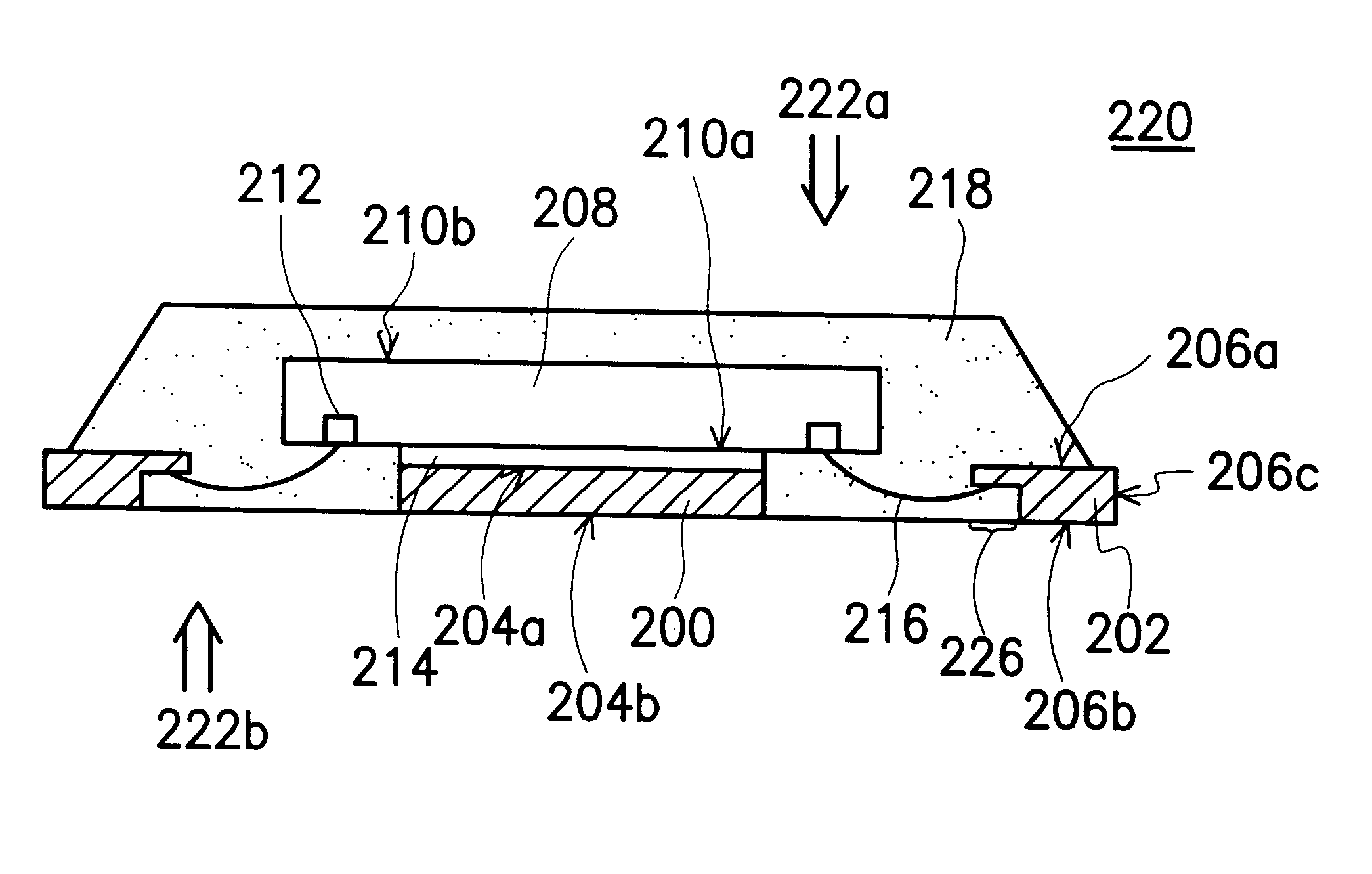
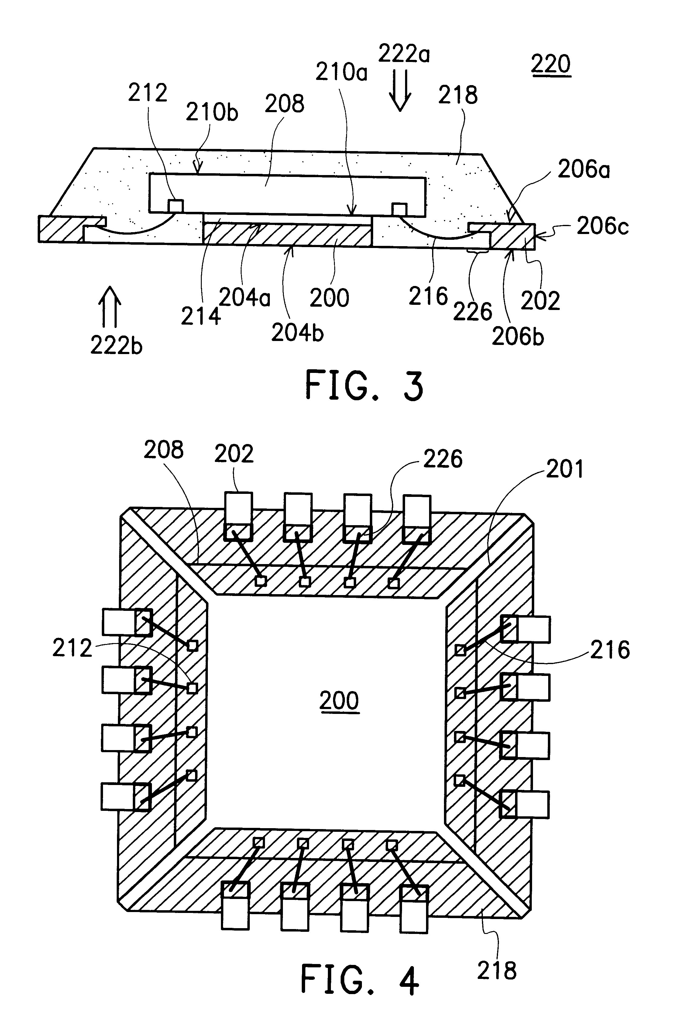
Shown in FIG. 3 is a cross-sectional view of a thermally enhanced quad flat nonlead package of the first preferred embodiment of the present invention while FIG. 4 is a bottom view corresponding to FIG. 3 of the present invention. As shown in FIG. 3. and FIG. 4, a thermally enhanced quad flat non-lead package of semiconductor of the present invention is constructed on a lead frame that is constituted by a die pad 200 and a of leads 202 disposed on the periphery of the lead frame. The die pad 200 has a first surface 204a and a second surface 204b while the lead 202 has a first surface 206a and a second surface 206b. The die pad 200 and the leads 202 are coplaner, that is, the second surface 204b of the die pad 200 and the second surface 206b of the leads 202 are coplaner wherein the die pad 200 is connected to the lead frame by a support bar 201. The chip 208 has an active surface 210a and a corresponding back surface 210b wherein a plurality of bonding pads 212 used for external con...


PUM


Abstract

A thermally enhanced quad flat non-lead package of semiconductor comprises a chip a plurality of leads, and a molding compound. The chip has its active surface bonded to the top surface of the die pad, and the area of the die pad is smaller than that of the chip in order to expose the bonding pads on the active surface of the chip. The leads are disposed at the periphery of the die pad wherein the bottom surface of the lead has a stepped structure with a relatively thin portion to form a wire-bonding protruded zone. A plurality of bonding wires is used to electrically connect the wire-bonding protruded zone of the leads to the bonding pads of the chip. The molding compound encapsulates the chip, bonding wires, the die pad, and a portion of the surface of the leads, but exposes the bottom surface of the die pad. In this way, the encapsulating process makes the side surface of the lead, and the portion excluding the wire-bonding protruded zone of the bottom surface of the lead exposed in order to make the lead become the external connecting points of the package structure.

Description

1. Field of the InventionThis invention relates to a "thermally enhanced quad flat non-lead package" of semiconductor., and more particularly to a "thermally enhanced quad flat non-lead package of semiconductor" for improving the heat-dissipating effect of the package.2. Description of Related ArtIn the information explosion of the world nowadays, the integrated circuit has become indispensable in our daily life, regardless of our daily life in food, clothing, lodging, transportation, education, and entertainment, the product assembled by various integrated circuit devices can be found everywhere. Following the evolution of the electronic technology, more sophisticate electronic products with user friendly and complicated functions are continuously progressing and changing. Nevertheless, in order to provide an ongoing convenience and comfortable usage, all the products are heading for the design trend of "Light, Thin, Short, and Small". In additions, the fabrication process of semic...

Claims


Application Information

Patent Timeline
Patent Type & Authority Patents(United States)
IPC IPC(8): H01L23/31H01L23/495H01L23/48H01L23/28
CPCH01L23/3107H01L23/4951H01L2224/06135H01L2224/32014H01L2224/48091H01L2224/48247H01L2224/4826H01L2224/49171H01L2924/01079H01L2924/14H01L2924/18165H01L2224/73265H01L2224/73215H01L2224/32245H01L2224/45124H01L2224/45144H01L24/49H01L24/48H01L2924/00014H01L2924/00H01L24/45H01L2224/32145H01L2224/05599
Inventor HUANG, CHIEN-PINGKO, ERIC
Owner SILICONWARE PRECISION IND CO LTD
Why Eureka
Try Eureka