Color filter image array optoelectronic microelectronic fabrication with three dimensional color filter layer and method for fabrication thereof

a technology of optoelectronic microelectronic fabrication and color filter layer, which is applied in the direction of originals for photomechanical treatment, instruments, optical elements, etc., can solve the problems of increasing complexity and integration of purely electronic microelectronic fabrication and optoelectronic microelectronic fabrication

Inactive Publication Date: 2001-03-13
TAIWAN SEMICON MFG CO LTD
View PDF12 Cites 22 Cited by
  • Summary
  • Abstract
  • Description
  • Claims
  • Application Information

AI Technical Summary

Benefits of technology

A second object of the present invention is to provide a method for forming a color filter image array optoelectronic microelectronic fabrication in accord with the first object of the present invention, where the color filter image array optoelectronic microelectronic fabrication is formed with enhanced optical resolution and enhanced optical stability.
A third object of the present invention is to provide a method for forming a color filter image array optoelectronic microelectronic fabrication in accord with the first object of the present invention and the second object of the present invention, which method is readily commercially implemented.
There is provided by the present invention a method for forming an image array optoelectronic microelectronic fabrication, where the image array optoelectronic microelectronic fabrication is formed with enhanced optical resolution and enhanced optical stability. The present invention realizes the foregoing objects by employing when forming the image array optoelectronic microelectronic fabrication at least a patterned first color filter layer which is registered with a first photoactive region within a substrate and encapsulated with a first optically transparent planarizing encapsulant layer prior to forming thereupon a patterned second color filter layer which is registered with a second photoactive region within the substrate and similarly encapsulated with a second optically transparent planarizing encapsulant layer.
The method of the present invention is readily commercially implemented. The present invention employs methods and materials as are generally known within, or at least readily adaptable to, the art of optoelectronic microelectronic fabrication, and more specifically to the art of image array optoelectronic microelectronic fabrication. Since it is at least in part a process control in conjunction with design considerations which provides the present invention, rather than the existence of methods and materials which provides the present invention, the method of the present invention is readily commercially implemented.

Problems solved by technology

While the level of complexity and integration of both purely electronic microelectronic fabrications and optoelectronic microelectronic fabrications continues to increase, fabrication of advanced optoelectronic microelectronic fabrications often provides unique fabrication challenges insofar as fabrication of advanced optoelectronic microelectronic fabrications requires attention to both the optical properties and the electrical properties of materials which are employed in forming such advanced optoelectronic microelectronic fabrications.

Method used


Image

  • Color filter image array optoelectronic microelectronic fabrication with three dimensional color filter layer and method for fabrication thereof
  • Color filter image array optoelectronic microelectronic fabrication with three dimensional color filter layer and method for fabrication thereof
  • Color filter image array optoelectronic microelectronic fabrication with three dimensional color filter layer and method for fabrication thereof

Examples


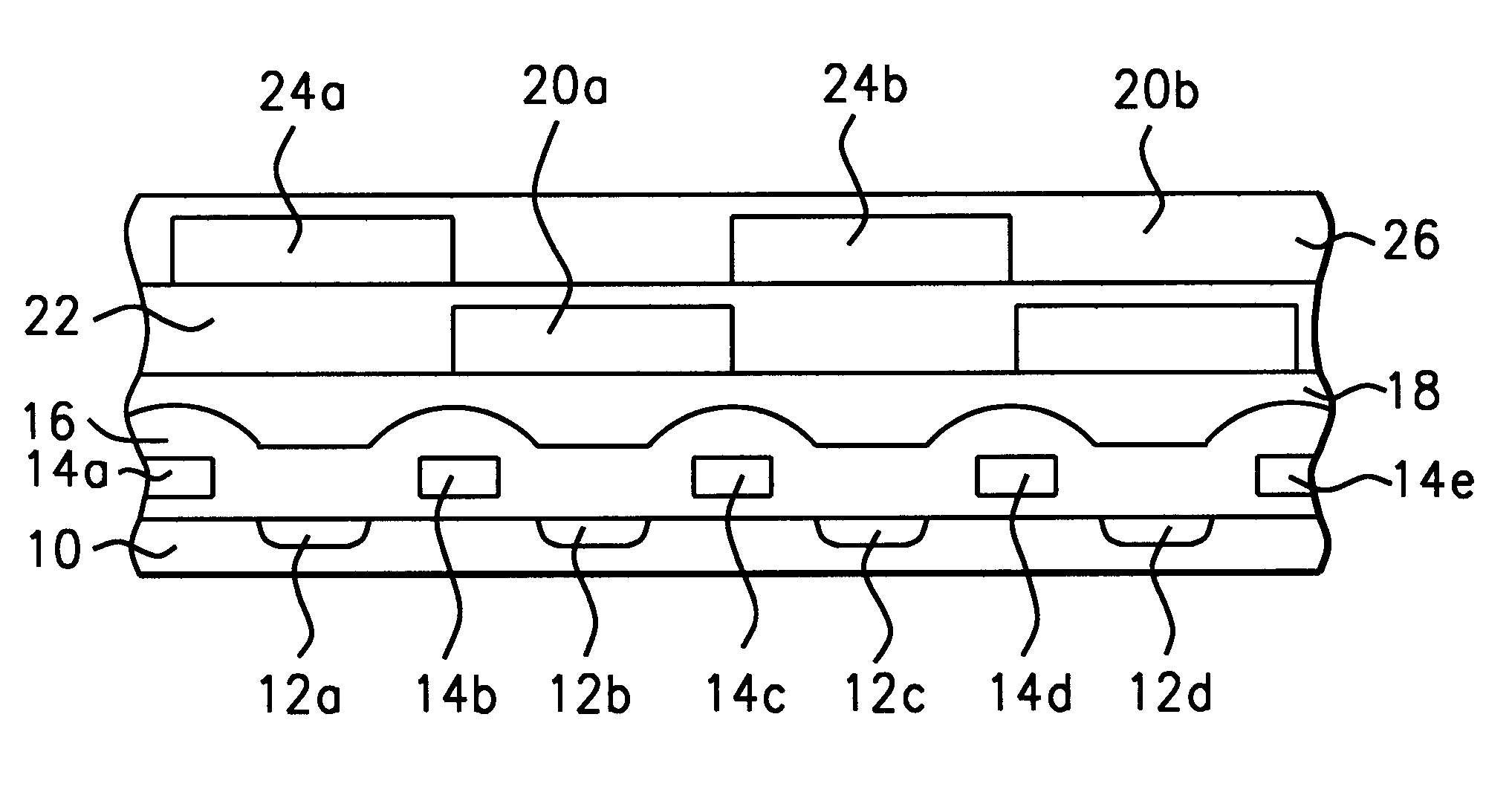
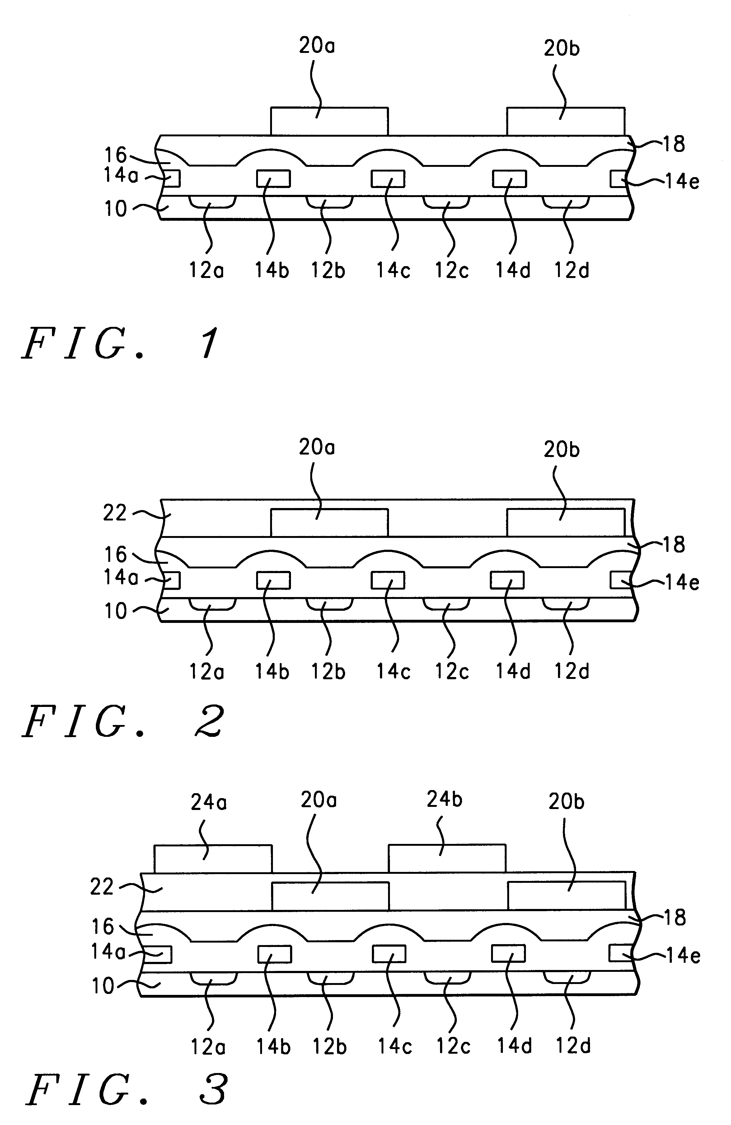
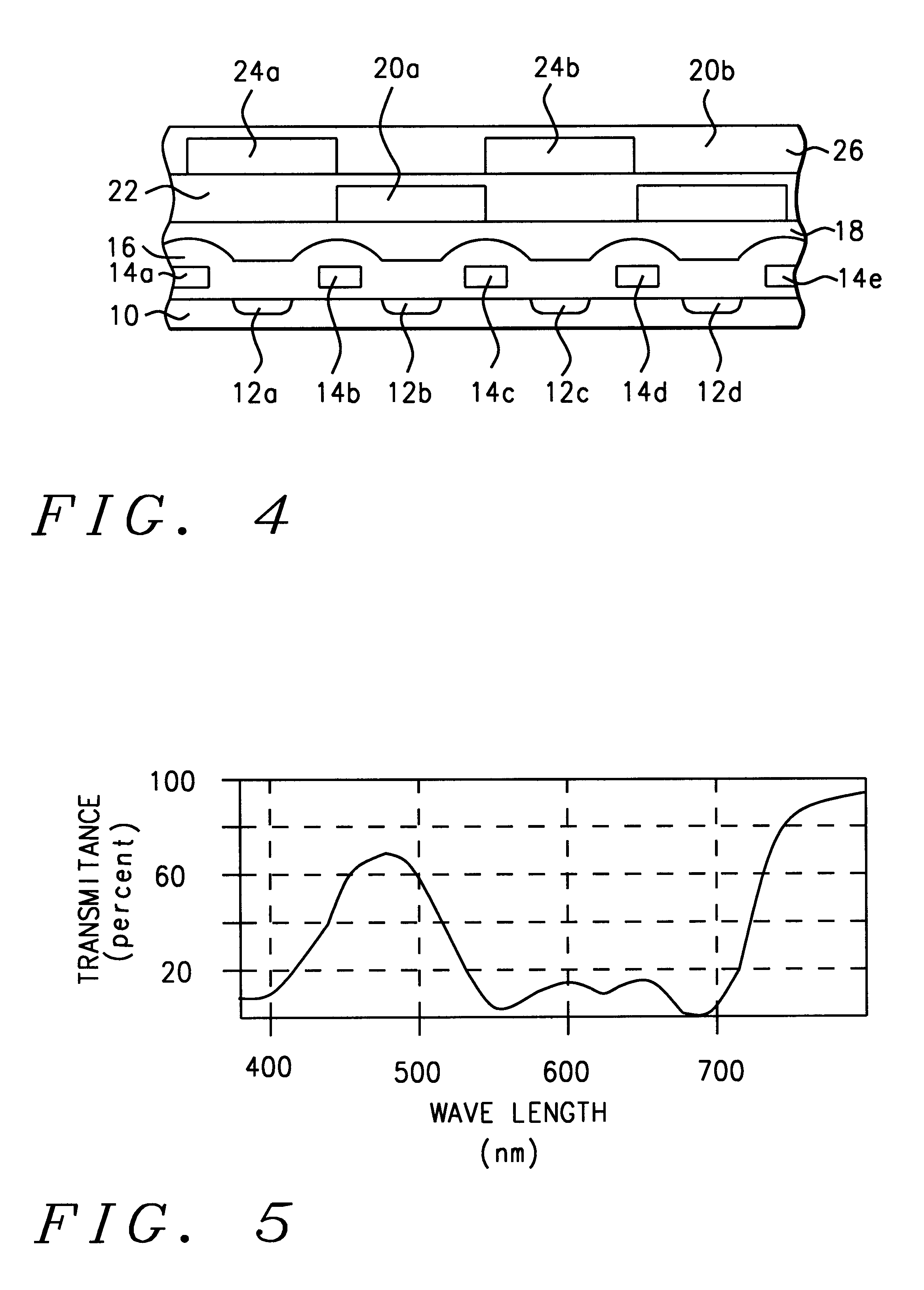
Embodiment Construction

There were obtained two quartz plates each of a real dimensions about 150 by about 150 millimeters and thickness dimension about 0.76 millimeters. There was then coated upon each of the two quartz plates a layer of product number CCD 186 positive photoresist material supplied by Polaroid Corporation, into which was incorporated a loading of a blue dye colorant material. Each of the two layers of positive photoresist material was coated and thermally cured at a temperature of about 100 degrees centigrade to provide a thickness of about 13000 angstroms. Each of the two layers of positive photoresist material was then exposed to a developer as is commonly employed to develop photoexposed portions of the positive photoresist material.

An optical transmission spectrum of one of the two developed positive photoresist layers was then obtained.

One of the two developed positive photoresist layers was then hardbaked at a temperature of about 220 degrees centigrade for a time period of about 6 ...


PUM


Abstract

A method for forming an optoelectronic microelectronic fabrication and an optoelectronic microelectronic fabrication fabricated in accord with the method. There is first provided a substrate having at minimum a first photoactive region and a second photoactive region formed therein. There is then formed over the substrate a patterned first color filter layer registered with the first photoactive region. There is then formed upon the patterned first color filter layer a first optically transparent planarizing encapsulant layer. There is then formed upon the first optically transparent planarizing encapsulant layer a patterned second color filter layer registered with the second photoactive region. Finally, there is then formed upon the patterned second color filter layer a second optically transparent planarizing encapsulant layer. The method contemplates an optoelectronic microelectronic fabrication fabricated in accord with the method.

Description

1. Field of the InventionThe present invention relates generally to methods for fabricating image array optoelectronic microelectronic fabrications. More particularly, the present invention relates to methods for fabricating with enhance optical resolution color filter image array optoelectronic microelectronic fabrications.2. Description of the Related ArtMicroelectronic fabrications are formed from microelectronic substrates over which are formed patterned microelectronic conductor layers which are separated by microelectronic dielectric layers. Within the general art of microelectronic fabrication, there exist microelectronic fabrications whose operation is based solely upon electrical signal storage and processing characteristics of microelectronic devices and microelectronic circuits formed upon a microelectronic substrate. Examples of such microelectronic fabrications typically include semiconductor integrated circuit microelectronic fabrications and ceramic substrate packagin...

Claims


Application Information

Patent Timeline
Patent Type & Authority Patents(United States)
IPC IPC(8): G02B5/20H01L31/0232H01L31/0216
CPCG02B5/201H01L31/0232H01L31/02162H01L31/02327H01L27/14621H01L27/14685
Inventor FAN, YANG-TUNGLEE, CHIH-HSIUNG
Owner TAIWAN SEMICON MFG CO LTD
Why Eureka
Try Eureka