Post deposition treatment of dielectric films for interface control

Inactive Publication Date: 2001-03-20
APPLIED MATERIALS INC
View PDF11 Cites 246 Cited by
  • Summary
  • Abstract
  • Description
  • Claims
  • Application Information

AI Technical Summary

Problems solved by technology

Unfortunately, the use of metal organic precursors tend to incorporate carbon into the deposited oxide.
Excess carbon is thought to lead to high leakage currents in metal oxide dielectrics.
Unfortunately, converting the amorphous metal dielectric to a polycrystalline dielectric in a high temperature oxygen anneal traps excess carbon in the dielectric film.
Additiona

Method used


Image

  • Post deposition treatment of dielectric films for interface control
  • Post deposition treatment of dielectric films for interface control
  • Post deposition treatment of dielectric films for interface control

Examples


Embodiment Construction

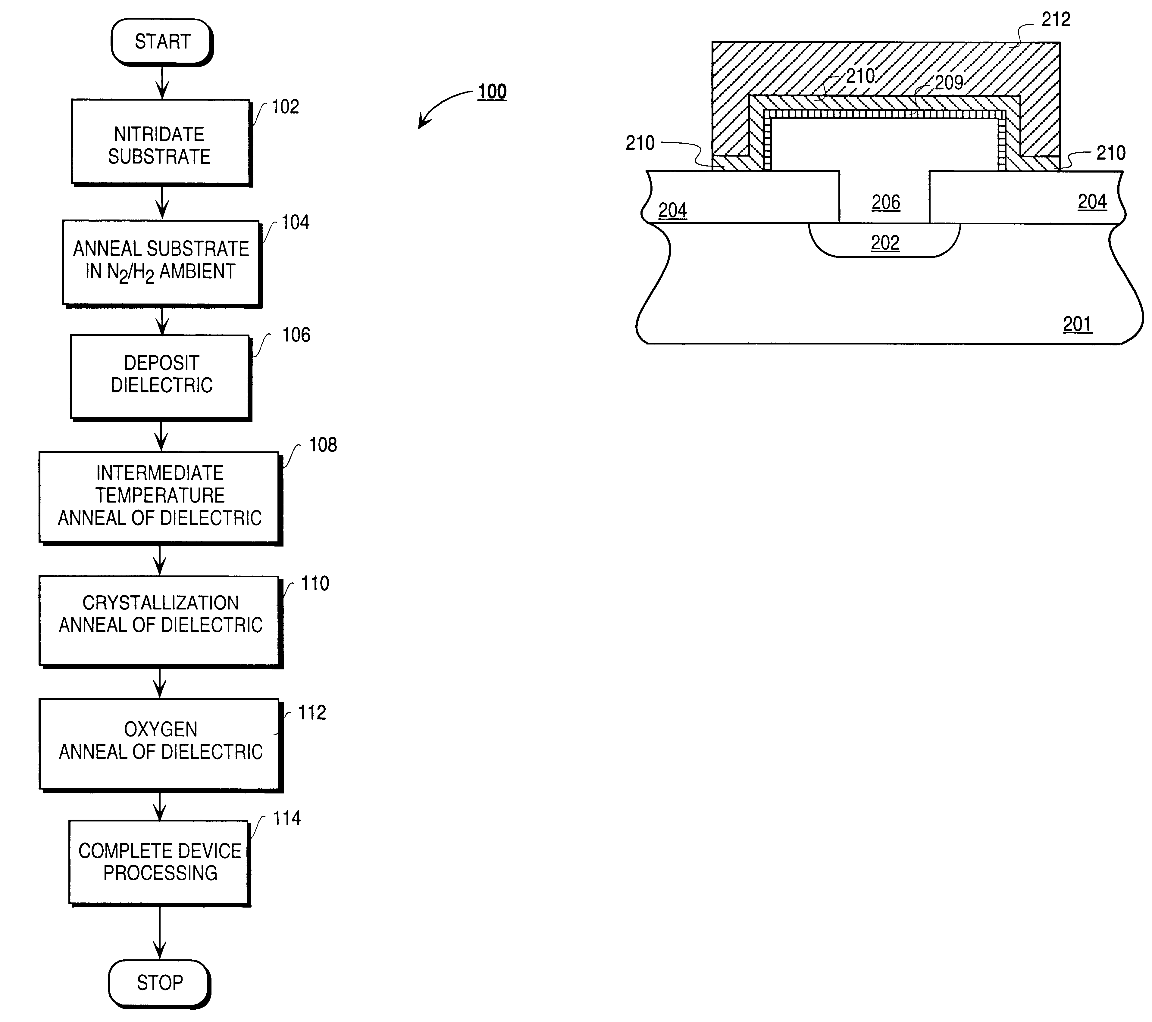
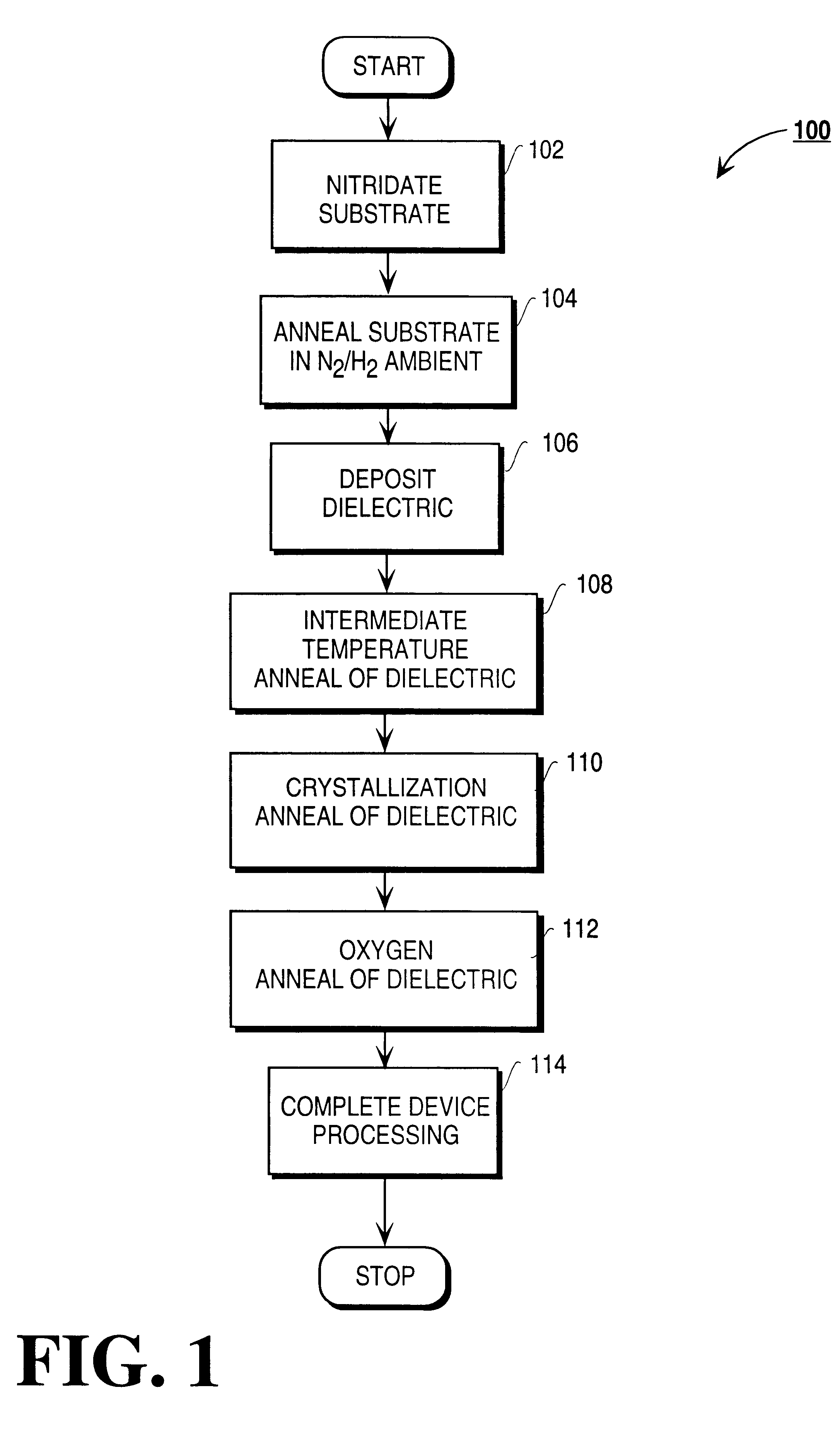
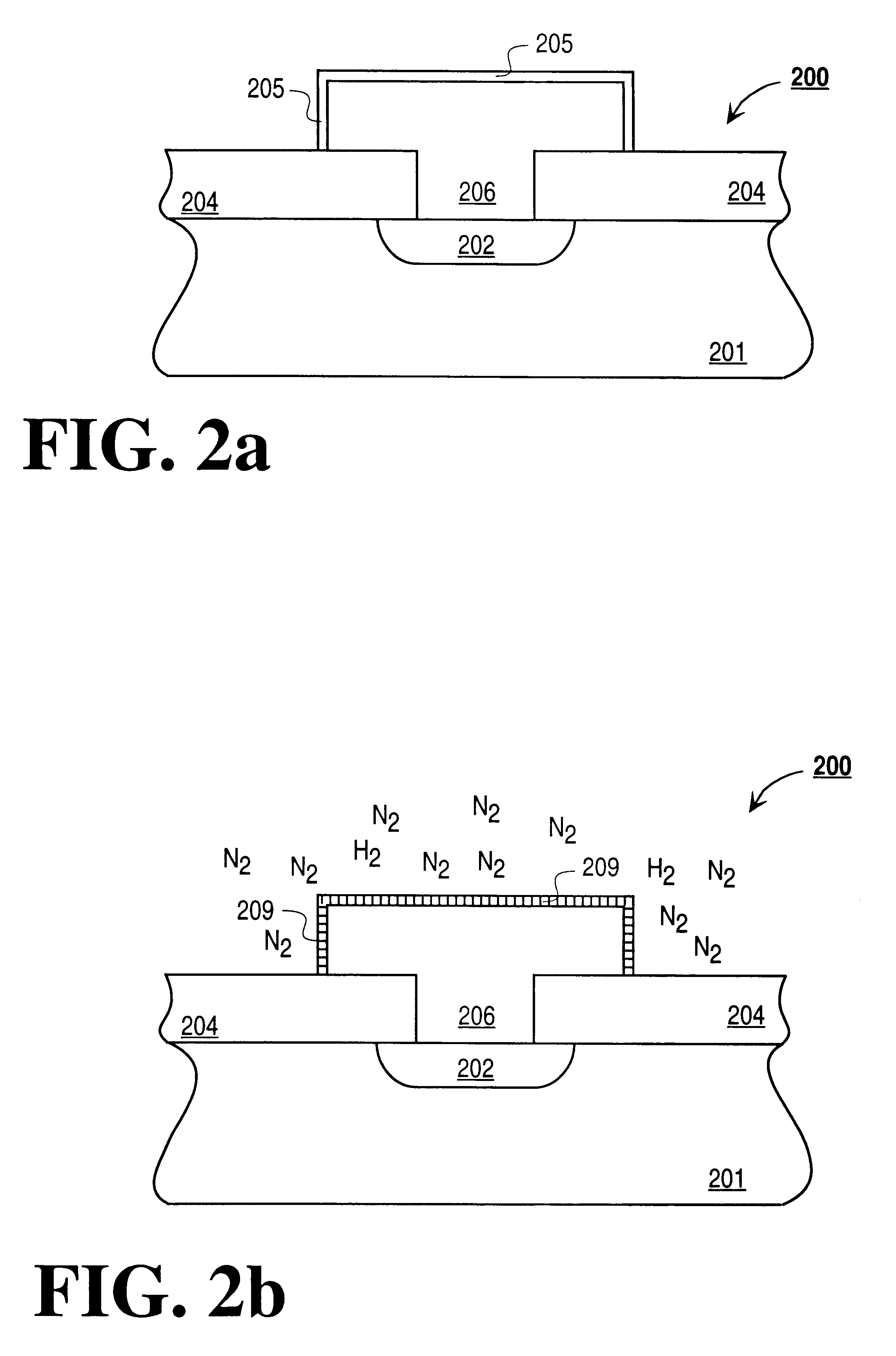
The present invention describes a novel method and apparatus for post treatment of a dielectric film for interface control. In the following description numerous specific details such as specific equipment, and process parameters are set forth in order to provide a thorough understanding of the present invention. One skilled in the art will appreciate the ability to use alternative configurations and process details to the disclosed specifics without departing from the scope of the present invention. In other instances, well known semiconductor processing equipment and methodology have not been described in detail in order to not unnecessarily obscure the present invention.

The post deposition treatment of the present invention is a series of anneal steps which together improve the interface characteristics and electrical properties of a deposited metal oxide dielectric film. According to the present invention, a metal oxide dielectric film, such as tantalum oxide or titanium oxide, ...


PUM


Abstract

A method of forming a metal oxide dielectric film. According to the present invention an amorphous metal oxide dielectric film is deposited over a substrate utilizing a metal organic precursor. The substrate is then heated in an inert ambient to convert the amorphous metal oxide dielectric to a polycrystalline metal oxide dielectric. The polycrystalline metal dielectric is then heated in a oxygen containing ambients.

Description

1. Field of the InventionThe present invention relates to the field of semiconductor manufacturing and more specifically to a method and apparatus for treating a deposited metal oxide dielectric film for interface control.2. Discussion of Related ArtIntegrated circuits are made up of literally millions of active and passive devices such as transistors, capacitors and resistors. In order to provide more computational power and / or more storage capability in an integrated circuit, device features are reduced or scaled down in order to provide higher packing density of devices. An important feature to enable scaling of devices is the ability to form high quality, high dielectric constant films for capacitor and gate dielectrics.High dielectric constant films are generally ceramic films (i.e., metal-oxides) such as tantalum pentaoxide, titanium oxide, BST, and PZT. These films are generally deposited in the amorphous state by thermal chemical vapor deposition utilizing a metal organic pr...

Claims


Application Information

Patent Timeline
IPC IPC(8): H01L21/02H01L21/28H01L29/51H01L29/40H01L21/8242H01L21/316H01L27/108
CPCH01J37/32862H01L21/28185H01L21/28194H01L21/28202H01L29/513H01L29/517H01L29/518H01L21/02172
Inventor NARWANKAR, PRAVIN K.SAHIN, TURGUTREDINBO, GREGORY F.LIU, PATRICIA M.TRAN, HUYEN T.
Owner APPLIED MATERIALS INC
Why Eureka
Try Eureka