Interconnection structure and process module assembly and rework

a technology of interconnection structure and process module, applied in the direction of printed circuit, sustainable manufacturing/processing, final product manufacturing, etc., can solve the problems of increasing the length of time, putting the interconnection structure out of alignment, and typical experien

Inactive Publication Date: 2001-05-22
ULTRATECH INT INC
View PDF17 Cites 57 Cited by
  • Summary
  • Abstract
  • Description
  • Claims
  • Application Information

AI Technical Summary

Problems solved by technology

As a result, during circuit card joining and reworking of these packages, two problems are typically experienced.
First, during joining, the solder composition attaching the columns to the substrate can melt causing the columns to tilt, thus, putting the interconnect structure out of alignment.
This is a labor intensive process that also critically increases the length of time that the card site must be kept within the temperature range necessary to facilitate removal of all the columns or balls (200-220.degree. C.
Repeated localized heating to pick up columns has led to circuit card land delaminations causing the entire card to be unusable.
Additionally, this problem will further develop as package sizes increase, and more columns or balls are added to the structure.
This prior art patent, however, does not address creating a transient liquid solder interface with fine metal powder additives, which after reflow and attachment to the substrate pads create a higher effective melting point interface.
This process, however, does not utilize a metal powder mixed in the interface solder, balls and columns, being joined to the substrate prior to any card attachment or rework.
However, there is no disclosure regarding changing the interface solder melting point by addition of high melting reacting powders.

Method used


Image

  • Interconnection structure and process module assembly and rework
  • Interconnection structure and process module assembly and rework
  • Interconnection structure and process module assembly and rework

Examples


Embodiment Construction

)

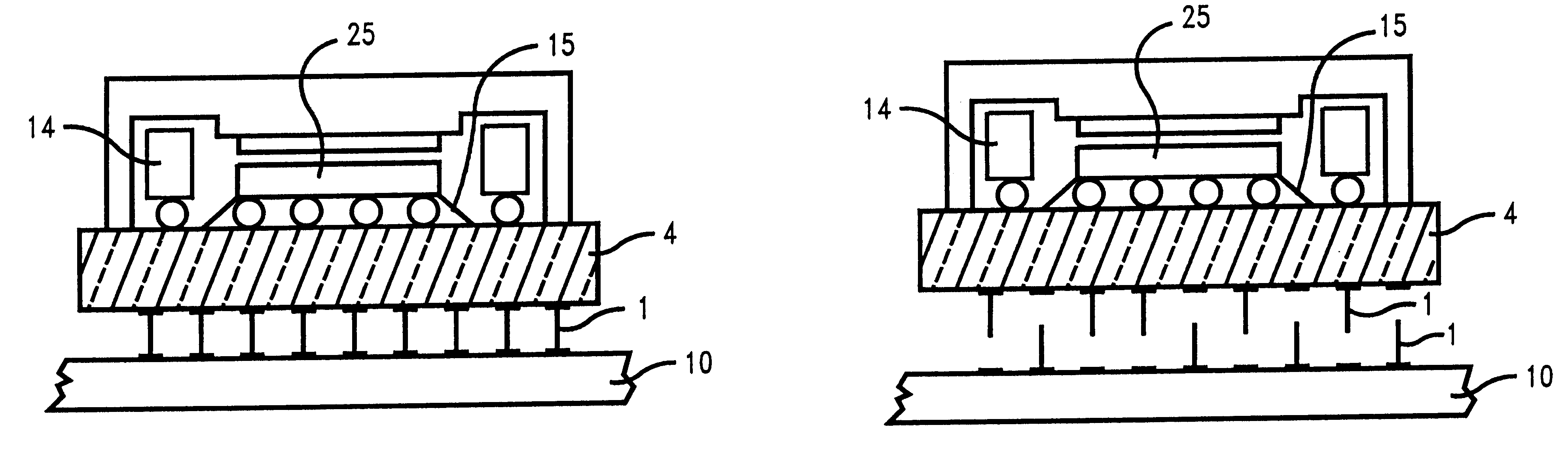
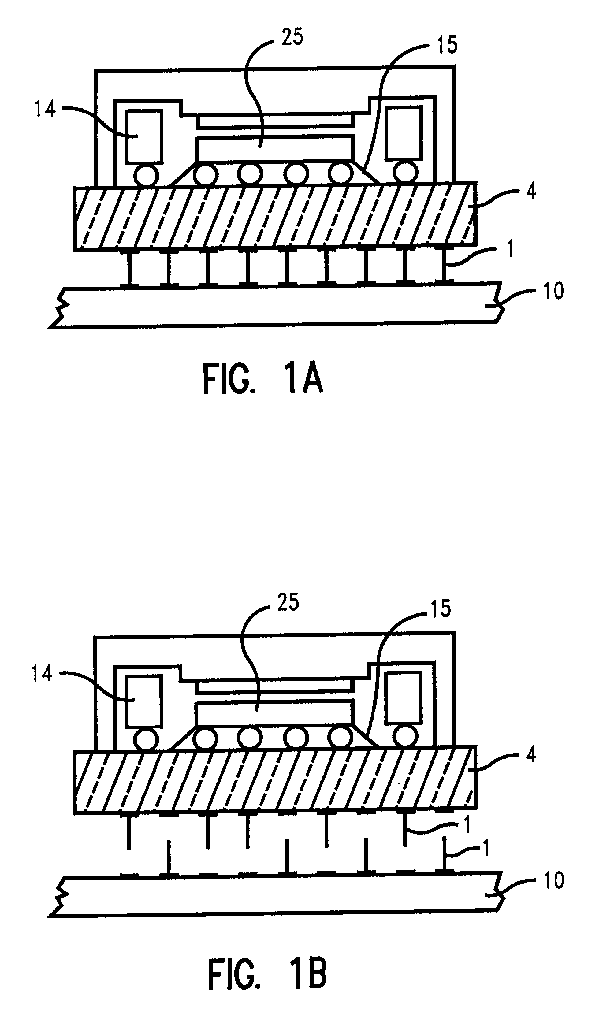
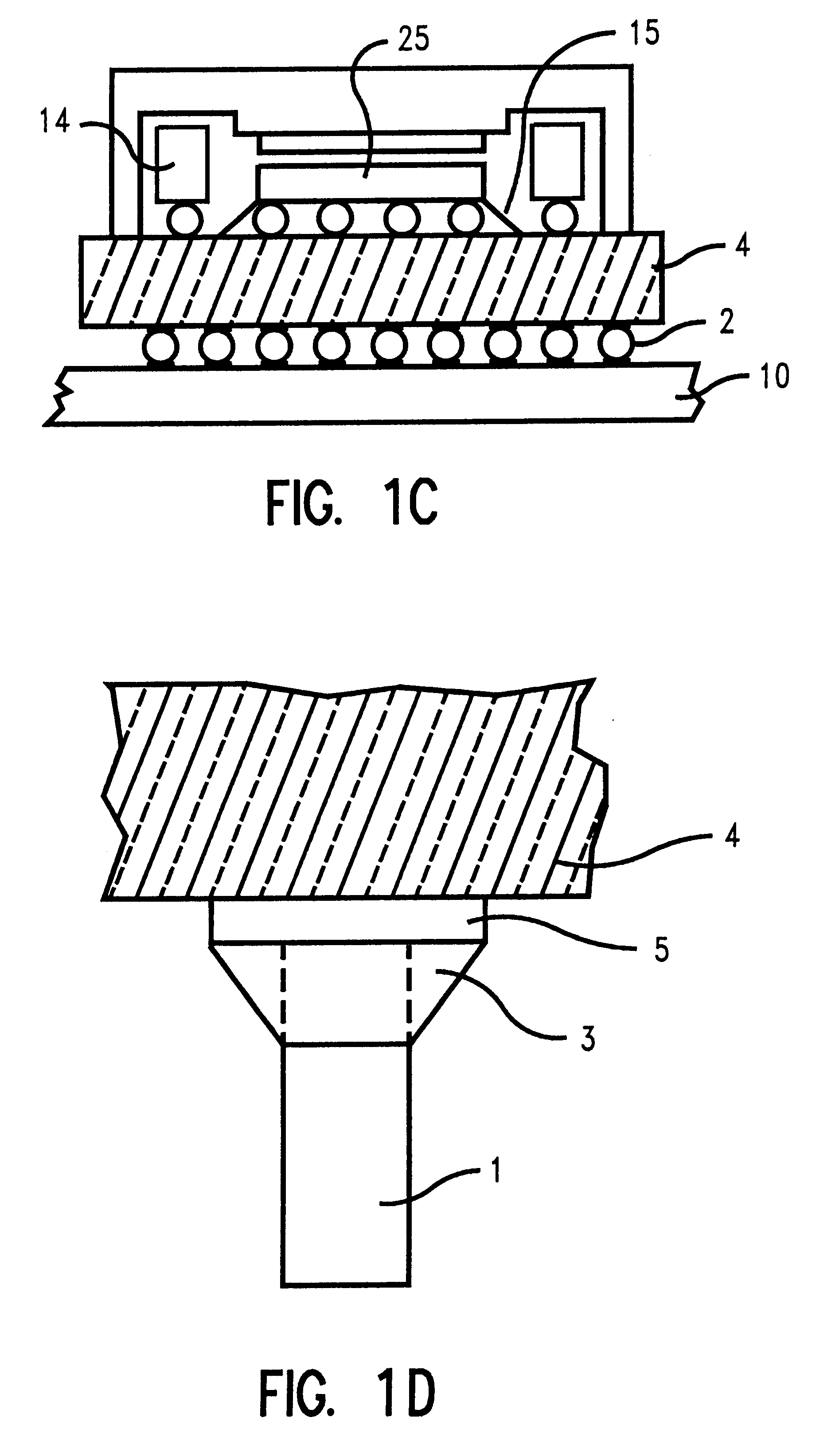
In describing the preferred embodiment of the present invention, reference will be made herein to FIGS. 1-9 of the drawings in which like numerals refer to like features of the invention. Features of the invention are not necessarily shown to scale in the drawings.

This invention relates to an interconnection structure and a process for making and detaching the same. Chiefly, of a surface mount column or ball grid array for formation of an interconnection structure between an electronic module assembly and circuit board. Column Grid Arrays (CGAs) are conventionally created by joining a high melting solder column to a substrate by means of a low-melting solder. Alternatively, they are created by casting a high melting solder directly onto external pads on the ceramic substrate body. The latter process has some desirable characteristics, in that the joint to the substrate is high melting, and does not reflow during the attachment of the module assembly to the card. The former also has...


PUM

PropertyMeasurementUnit
temperatureaaaaaaaaaa
temperaturesaaaaaaaaaa

Abstract

An interconnection structure and methods for making and detaching the same are presented for column and ball grid array (CGA and BGA) structures by using a transient solder paste on the electronic module side of the interconnection that includes fine metal powder additives to increase the melting point of the solder bond. The metal powder additives change the composition of the solder bond such that the transient melting solder composition does not completely melt at temperatures below +230° C. and detach from the electronic module during subsequent reflows. A Pb-Sn eutectic with a lower melting point is used on the opposite end of the interconnection structure. In the first method a transient melting solder paste is applied to the I / O pad of an electronic module by a screening mask. Interconnect structures are then bonded to the I / O pad. In a second method, solder preforms in a composition of the transient melting solder paste are wetted onto electronic module I / O pads and interconnect columns or balls are then bonded. Detachment of an electronic module from a circuit card can then be performed by heating the circuit card assembly to a temperature above the eutectic solder melting point, but below the transient solder joint melting point.

Description

1. Field of the InventionThe present invention relates generally to a new interconnection and a method for making and detaching the same, and more particularly, to a solder connection. This invention addresses the card assembly / rework issues associated with column and ball grid array (CGA and BGA) structures by introducing an interconnection structure with a transient liquid solder interface that includes fine metal powder additives.2. Description of Related ArtCeramic column grid array (CGA) packages are being used for many high performance ASIC chips and microprocessor chips for IBM and original engineering manufacturer (OEM) customers. The preferred processes for lowest cost manufacturing and minimum handling damage during bond, assembly, and test are the wire CGA process and the ball grid array (BGA) process. However, inherent to the joining process of the wire CGA and BGA structure is an eutectic interface used in the column or ball attachment to the substrate pads. As a result...

Claims


Application Information

Patent Timeline
Patent Type & Authority Patents(United States)
IPC IPC(8): H01L21/48H01L23/498H01L21/02H01L23/48H05K3/34H01L23/32
CPCH01L21/4853H05K3/3436H01L23/49811Y10T29/49126H01L2224/16225H01L2224/73253H01L2924/01046H01L2924/01078H01L2924/15311H01L2924/15312H01L2924/16152H01L2924/19105H05K3/3463H05K3/3484H05K2201/0215H05K2201/0272H05K2201/094H05K2201/10992H05K2203/041H05K2203/0415H01L2924/01322H01L2924/01327H01L2924/00H05K3/3485Y02P70/50
Inventor FAROOQ, SHAJIINTERRANTE, MARIO J.RAY, SUDIPTA K.SABLINSKI, WILLIAM E.
Owner ULTRATECH INT INC
Why Eureka
Try Eureka