Field effect transistor having a floating gate

a field effect transistor and floating gate technology, applied in the direction of basic electric elements, semiconductor devices, electrical equipment, etc., can solve the problems of metallization, lithographic patterning and reactive ion metal etching, which are quite difficult to perform on a non-planar gate surfa

Inactive Publication Date: 2001-06-12
GLOBALFOUNDRIES INC
View PDF34 Cites 190 Cited by
  • Summary
  • Abstract
  • Description
  • Claims
  • Application Information

AI Technical Summary

Problems solved by technology

However, incorporating this technology into a logic application presents problems for metallization due to the topography, especially when wiring dimensions become less than 0.25 microns.
Lithographic patterning and reactive ion metal etching both are quite difficult to perform on a non-planar gate surface.

Method used


Image

  • Field effect transistor having a floating gate
  • Field effect transistor having a floating gate
  • Field effect transistor having a floating gate

Examples


Embodiment Construction

Reference to the figures will facilitate an understanding of the present invention.

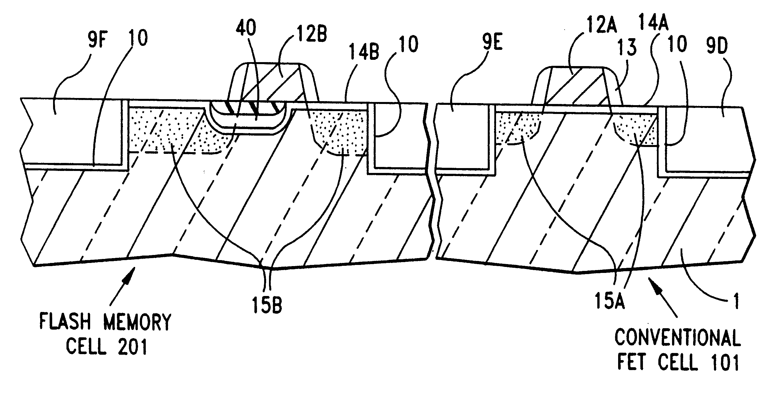
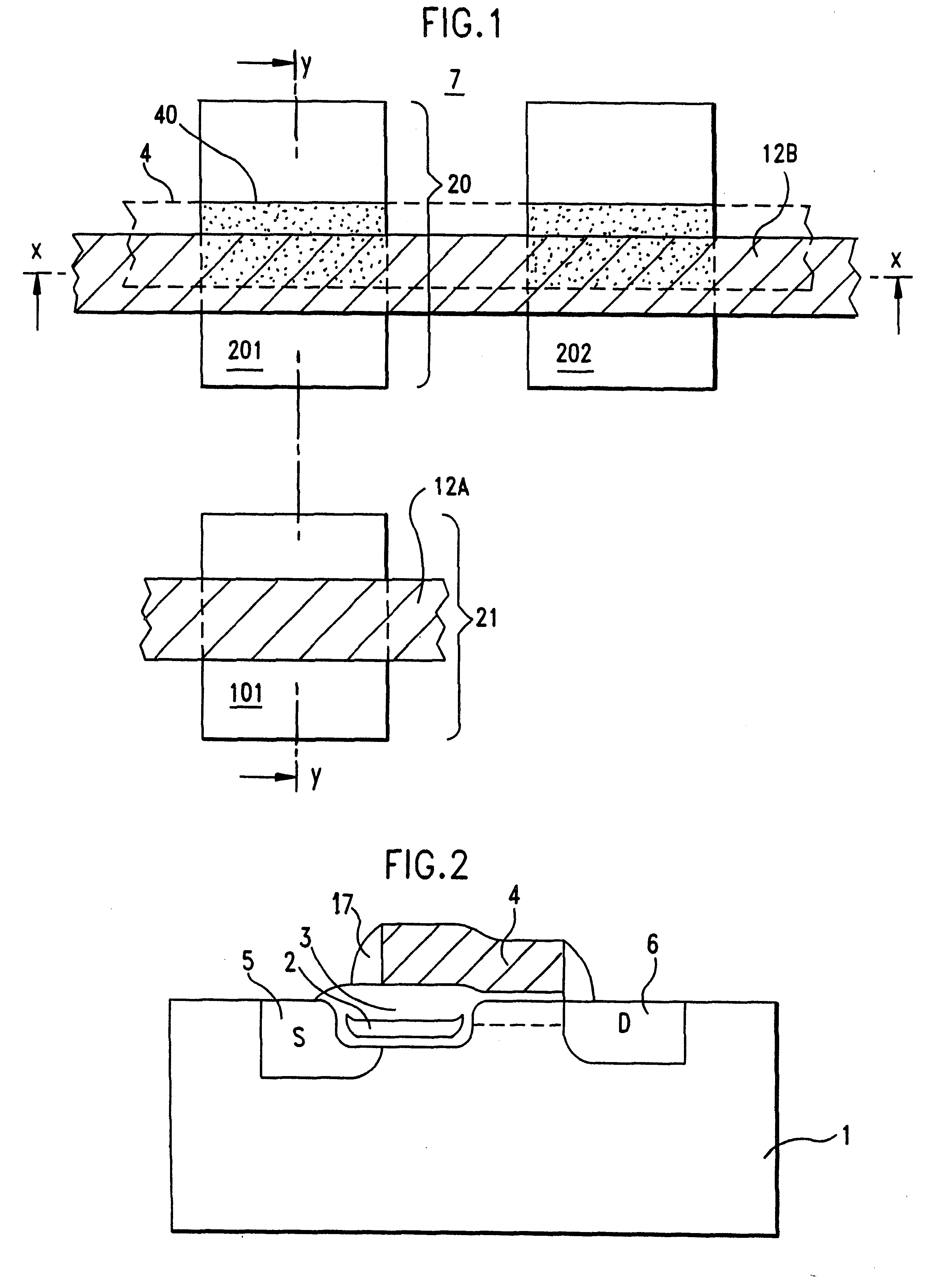
FIG. 1 schematically illustrates a top view of flash memory cells 201 and 202 in accordance with the present invention along with a conventional FET device 101. FIG. 2 is a schematic diagram of a split gate arrangement in accordance with the present invention. In FIG. 2, numeral 1 represents the semiconductor substrate, numeral 2 illustrates the floating gate recessed into the substrate 1, numeral 3 represents the gate isolation for both the floating gate 2 and control gate 4, and numeral 17 represents sidewall isolation for the control gate. Numerals 5 and 6 represent source and drain regions respectively.

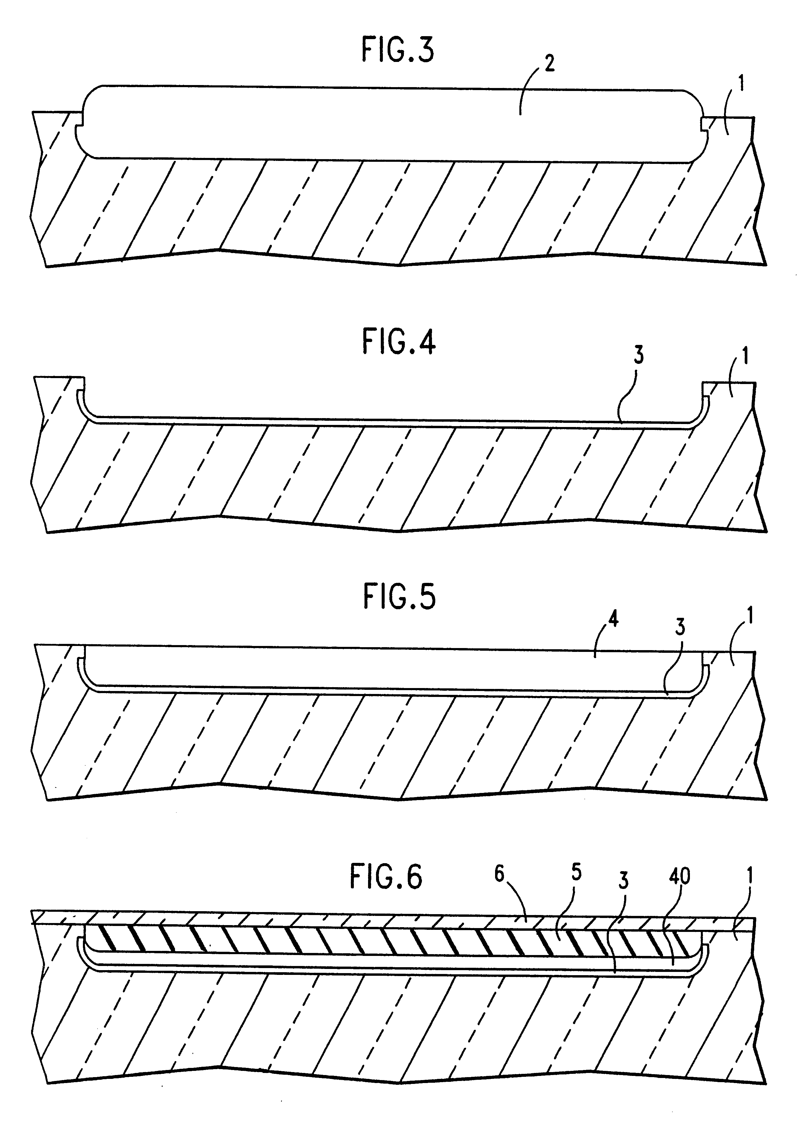
According to the present invention, recessed oxidation can be carried out by forming a layer of thermal oxide 2 on semiconductor substrate 1 (see FIGS. 3 and 10) using a mask such as a silicon nitride mask (not shown). The semiconductor substrate is typically silicon but can be any other semiconduct...


PUM


Abstract

A field effect transistor which comprises a semiconductor substrate having a source region and a drain region separated by a channel region; a conductive floating gate formed over a first portion of the channel region adjacent to the doped source region and recessed into the semiconductor substrate; and being separated from the first portion of the channel region by a first insulation layer; and a conductive control gate formed substantially over but electrically isolated from the floating gate and formed over the entire channel region; along with a method for fabricating such is provided.

Description

The present invention is concerned with a field effect transistor (FET) having a floating gate and especially flash memory cell structures exhibiting high programming efficiency. Furthermore, the present invention is concerned with a process for fabricating the FET structure of the present invention, and is especially concerned with a process for creating a split gate flash memory cell wherein the floating gate is recessed into the silicon substrate.BACKGROUND OF INVENTIONField effect transistors (FETs) employing a so-called "floating gate" along with a control gate are well known. The floating gate differs from a control gate in that it has no direct electrical connection to any external component and is surrounded by isolation on all sides. The presence of the control gate enables the device to function as a regular FET, while the floating gate collects and stores injected electrons or holes. The floating gate provides a method for changing the threshold voltage needed to pass a c...

Claims


Application Information

Patent Timeline
Patent Type & Authority Patents(United States)
IPC IPC(8): H01L21/70H01L21/28H01L21/02H01L21/8247
CPCH01L21/28273H01L27/11526H01L27/11543H01L29/40114H10B41/48H10B41/40
Inventor HSU, LOUIS L.MANDELMAN, JACK A.HU, CHIH-CHUN
Owner GLOBALFOUNDRIES INC
Why Eureka
Try Eureka