Voltage detection circuit power-on/off reset circuit and semiconductor device

a voltage detection circuit and power-on/off reset technology, applied in the direction of current/voltage detection, instruments, pulse techniques, etc., can solve the problems of difficult to properly terminate a sequence in operation, the memory data is destroyed in the memory circuit when the operation is immediately suspended, so as to prevent the wrong operation of non-volatile memory and stable voltage detection signal

Inactive Publication Date: 2001-06-12
RPX CORP
View PDF29 Cites 2 Cited by
  • Summary
  • Abstract
  • Description
  • Claims
  • Application Information

AI Technical Summary

Benefits of technology

The power-on / off reset circuit of claim 15 comprises a voltage detection circuit which detects a first voltage and a second voltage higher than the first voltage and outputs a first signal, wherein the first signal is transmitted at the second voltage when a power-supply voltage rises, and transmitted at the first voltage when the power-supply voltage drops, and a new operational sequence is prevented when the power-supply voltage is equal to or lower than the voltage for the first signal to be transmitted.
The inventions of claims 1-8 and 14 are voltage detection circuits which reduce the peak of the current drain and obtain a stable voltage detection signal. There is another effect that the stable voltage detection signal can be obtained even at a low voltage of turning on the power-supply.
The inventions of claims 18, 19, 20, and 21 have an effect of obtaining an operation stable against the fluctuation of the power-supply voltage by applying voltage hysteresis to the power-on / off reset voltage, thereby preventing the wrong operation of the non-volatile memory which is under the control of this signal.

Problems solved by technology

On the other hand, when a predetermined voltage is detected by the voltage detection circuit, a power-on / off reset circuit for immediately suspending the operations of the devices such as a logic circuit or a memory circuit might destroy memory data in the memory circuit when the operation is immediately suspended.
For this reason, it is difficult to properly terminate a sequence in operation.

Method used


Image

  • Voltage detection circuit power-on/off reset circuit and semiconductor device
  • Voltage detection circuit power-on/off reset circuit and semiconductor device
  • Voltage detection circuit power-on/off reset circuit and semiconductor device

Examples


embodiments 1

(Embodiments 1)

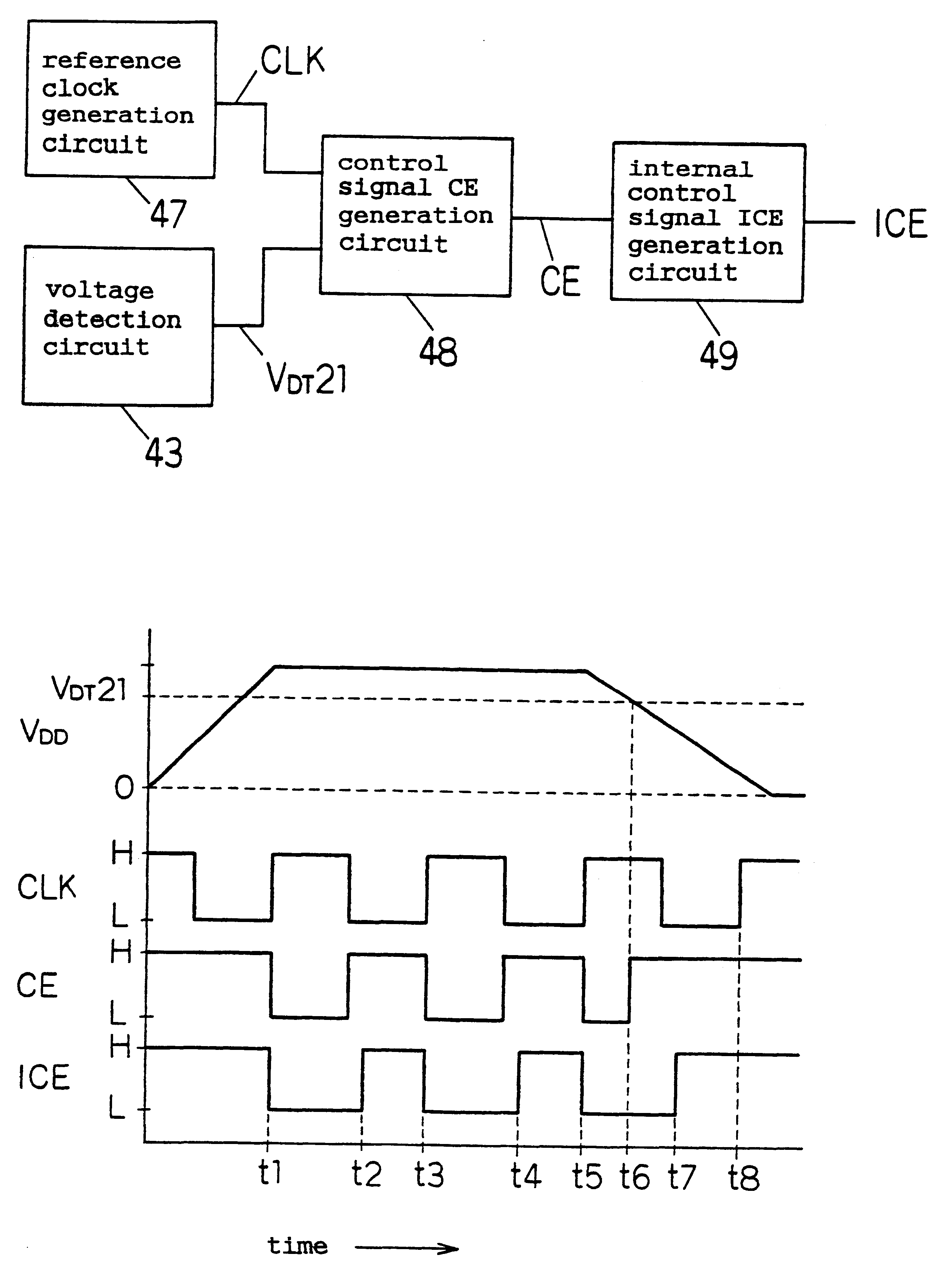
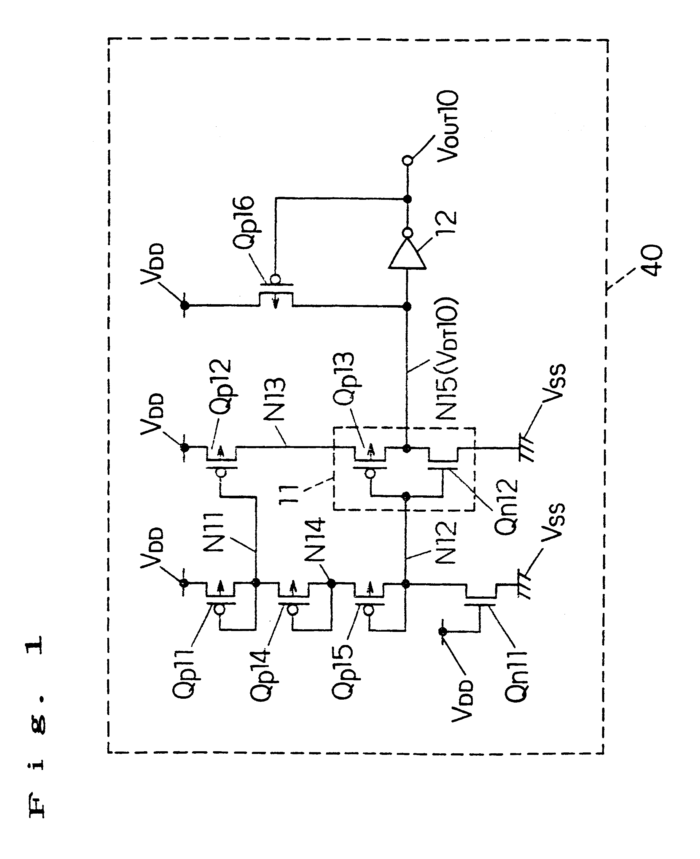
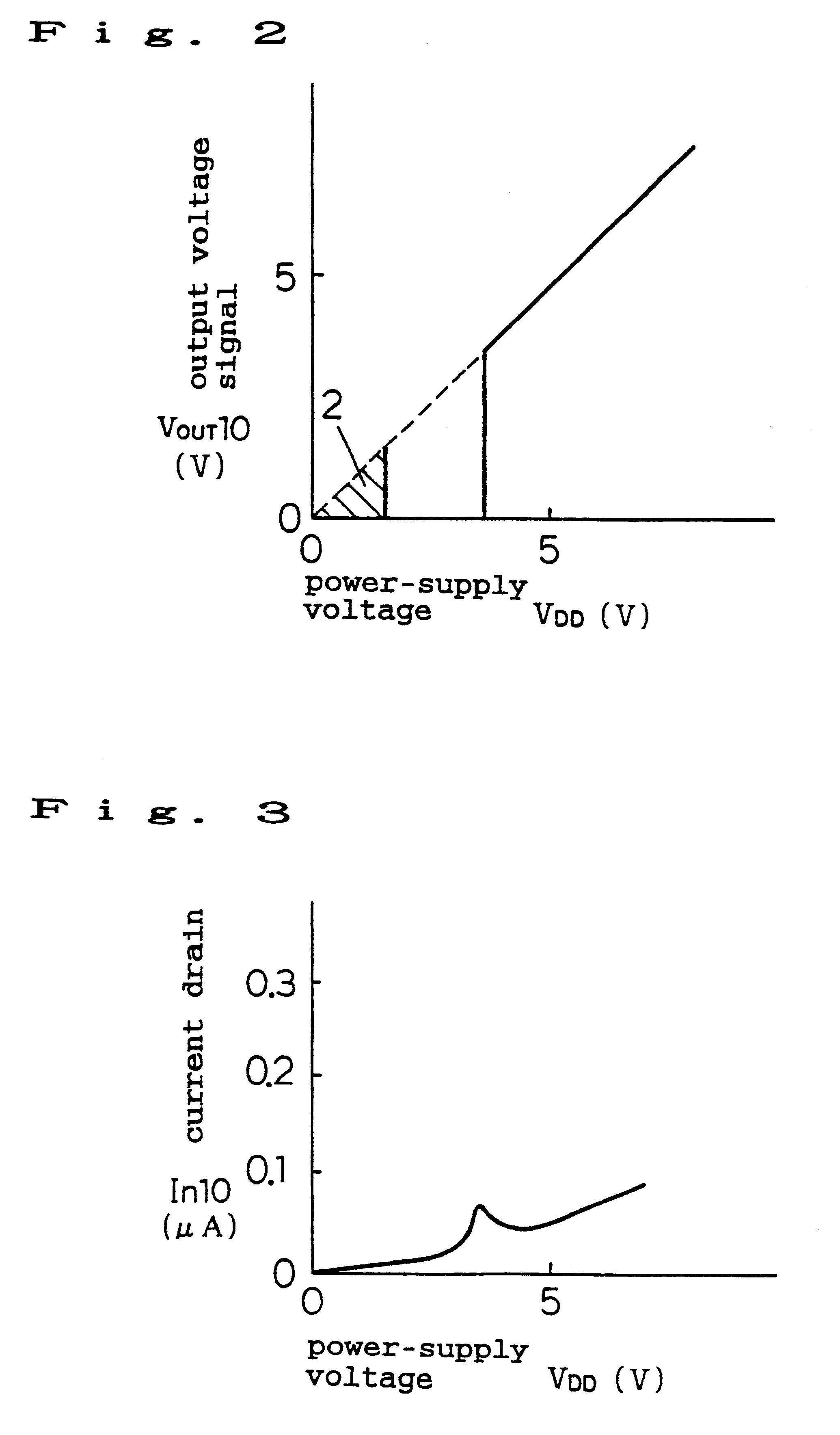
FIG. 1 shows the construction of the voltage detection circuit of the first embodiment of the present invention (corresponding to claims 1, 2, and 3). FIG. 2 shows the relationship between the power-supply voltage and the output voltage signal, and FIG. 3 shows the relationship between the power-supply voltage and the current drain.

The construction of the present embodiment will be explained hereinafter. In FIG. 1, Qp 11-Qp 16 are P-channel type MOS transistors, Qn 11 and Qn 12 are N-channel type MOS transistors, and 11 and 12 are NOT circuits.

The source of the P-channel type MOS transistor Qp 11 is connected with the power-supply voltage VDD, and its gate and drain are connected with the node N 11. The source of the P-channel type MOS transistor Qp 12 is connected with the power-supply voltage VDD, and its gate and drain are connected with the node N 11 and the node N 13, respectively. The P-channel type MOS transistors Qp 14 and Qp 15 are connected with each other i...

embodiment 2

(Embodiment 2)

FIG. 4 shows the construction of the voltage detection circuit of the second embodiment of the present invention (corresponding to claim 4).

In the present embodiment, a voltage detection circuit 41 which can detect a lower voltage than in the first embodiment is added, the output signal VDT 20 whose logical voltage is "H" is supplied to the gate of the P-channel type MOS transistor Qp 17 at the low voltage of the voltage detection circuit 41, and this transistor Qp 17 is connected between the node N 15 and the power-supply voltage VDD. The present embodiment can prevent the circuit of FIG. 1 from becoming unstable at around 1.5V shown in FIG. 2.

As a result, this circuit can achieve a stable operation at a low voltage especially when the power supply is turned on, by means of a signal from a voltage detection circuit which detects a lower voltage than the voltage of the circuit itself.

embodiment 3

(Embodiment 3)

FIG. 5 shows the construction of the voltage detection circuit of the third embodiment of the present invention (corresponding to claims 5 and 6) , and FIG. 6 shows the waveform of the output signal when the power supply is turned on.

The present embodiment can be used in the voltage detection circuit 41 of the second embodiment.

The sources of the P-channel type MOS transistors Qp 21-Qp 24, the gates of the transistors Qp 21 and Qp 24 are connected with the power-supply voltage VDD. The drains of the transistors Qp 21-Qp 22 and the gates of the transistors Qp 22-Qp23 are connected with the node N 21. The drains of the transistors Qp 23-Qp24 are connected with the node N 23. The source of the P-channel type MOS transistor Qp 25 is connected with the node N 21, and its gate and drain are connected with the node N 22. A resistance R 21 is connected between the node N 22 and the ground voltage VSS. The N-channel type MOS transistor Qn 21 whose gate is the node N 23 is conne...


PUM


Abstract

The present invention comprises a first MOS transistor whose gate and drain are connected with a first node, a second MOS transistor whose gate and drain are connected with the first node and a third node, respectively, a first resistive element which is connected between the first node and a second node, a second resistive element which is connected between the second node and a ground voltage terminal, a first NOT circuit whose input terminal is connected with the second node, whose output terminal is a fourth node, and which is connected between the third node and the ground voltage terminal, and a second NOT circuit whose input terminal is connected with the fourth node and whose output terminal is a fifth node. Consequently, the present invention can detect voltage in a stable condition with low power consumption.

Description

The present invention relates to a voltage detection circuit for detecting a power-supply voltage or the like, a power-on / off reset circuit, and a semiconductor device.Recently, a technique has become popular for operating a semiconductor device in a stable condition in a wide power-supply voltage range by changing the internal circuit operation in accordance with the power-supply voltage value. For this reason, a voltage detection circuit for detecting a power-supply voltage value has become important.A conventional voltage detection circuit will be explained hereinafter with reference to FIGS. 23-25. FIG. 23 shows the construction of the conventional voltage detection circuit. FIG. 24 shows the relationship between the power-supply voltage and the output voltage signal in the conventional voltage detection circuit. FIG. 25 shows the relationship between the power-supply voltage and the current drain.Firstly, the circuit construction will be explained. As shown in FIG. 23, the Qp 6...

Claims


Application Information

Patent Timeline
Patent Type & Authority Patents(United States)
IPC IPC(8): G01R19/00G01R19/165G01R19/155G01R19/145G06F1/28G11C8/08G11C8/00G11C5/14G11C11/22H03K17/22
CPCG01R19/0084G01R19/155G01R19/16538G06F1/28G11C5/143G11C8/08G11C11/22H03K17/223G01R19/00
Inventor HIRANO, HIROSHIGEASARI, KOUJISUMI, TATSUMI
Owner RPX CORP
Why Eureka
Try Eureka