Device for imaging radiation

Inactive Publication Date: 2001-06-26
SIEMENS AG
View PDF6 Cites 50 Cited by
  • Summary
  • Abstract
  • Description
  • Claims
  • Application Information

AI Technical Summary

Benefits of technology

In accordance with a first aspect of the invention, there is provided an imaging device for radiation imaging, said device comprising an array of detector cells for generating a charge in response to incident radiation, an array of cell circuits for accumulating charge generated, and co

Problems solved by technology

However, if the imaging system is designed for high resolution, the data bandwidth for a live image at, for example, 30 frames per second may be so high that the requirements for the readout electronics for handling the data stream may become unreasonable.
A readout system fast enough to capture and process the images could become unreasonably expensive compared to the total cost of the imaging system.
Anothe

Method used


Image

  • Device for imaging radiation
  • Device for imaging radiation
  • Device for imaging radiation

Examples


Embodiment Construction

Exemplary embodiments are described by way of example only with reference to the accompanying drawings.

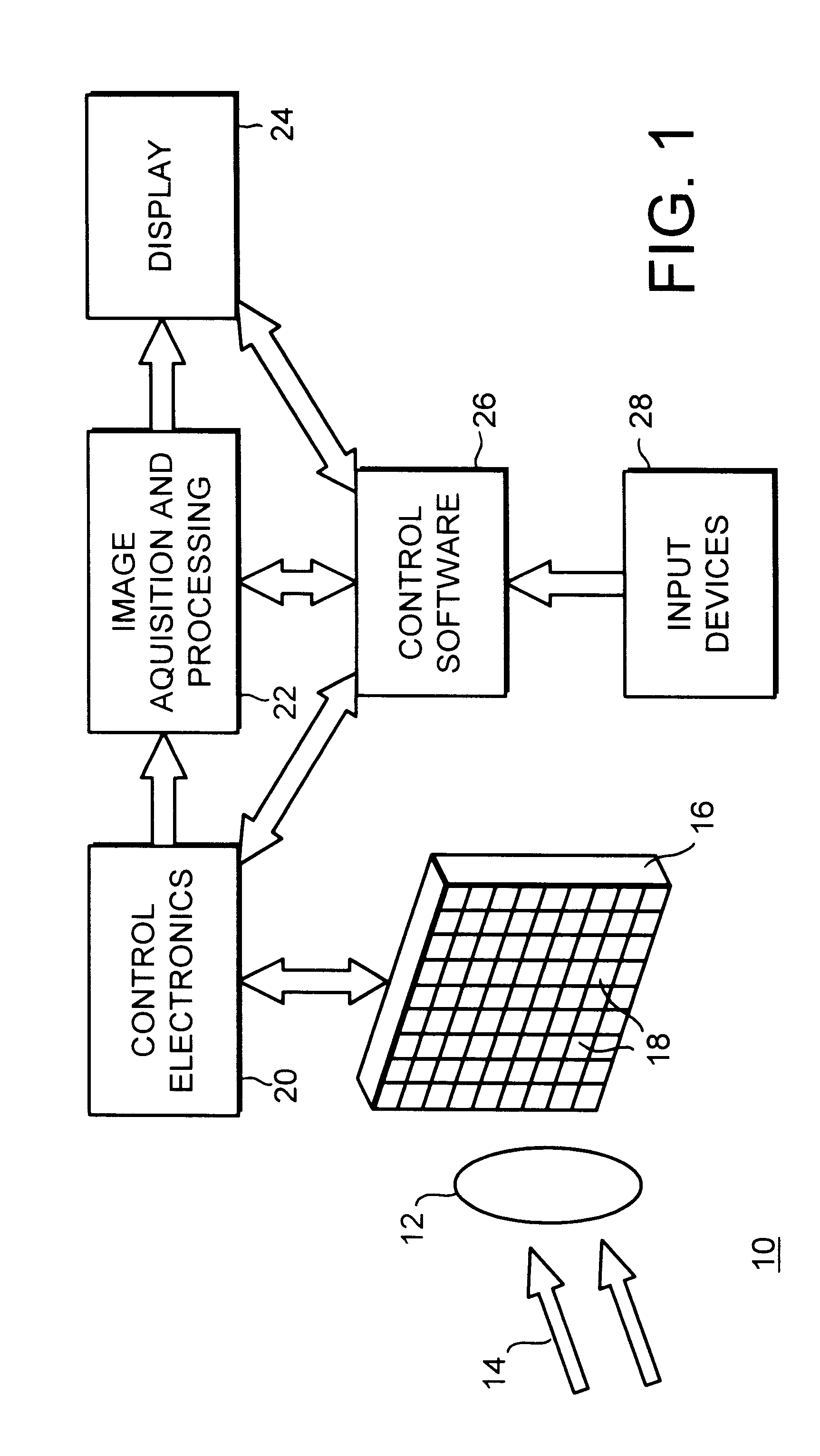
FIG. 1 shows an example of an imaging system for radiation imaging including an imaging device according to the invention. The imaging device is intended for imaging of high-energy radiation, for example X-ray radiation. However, the invention is not limited to imaging of high-energy X-ray radiation, but can be applied to detection of any type of radiation, for example a-ray, b-ray, g-ray, infra red or optical radiation, subject to choice of appropriate semiconductor substrate for the detector.

The imaging system 10 in FIG. 1 provides imaging of an object 12 subject to radiation 14. The object may, for example, be part of a human body in case of medical imaging or any other object, in case of non-destructive testing.

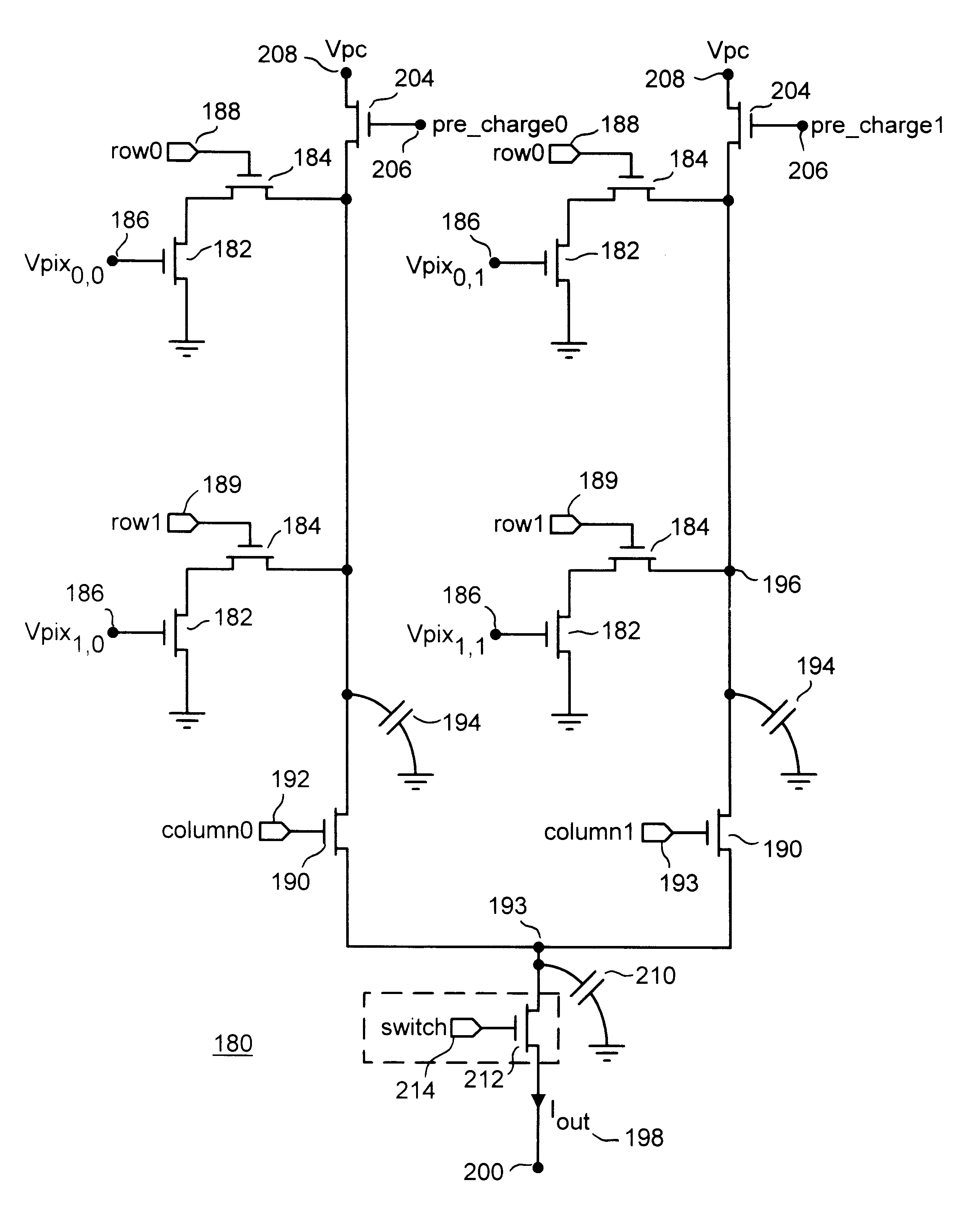
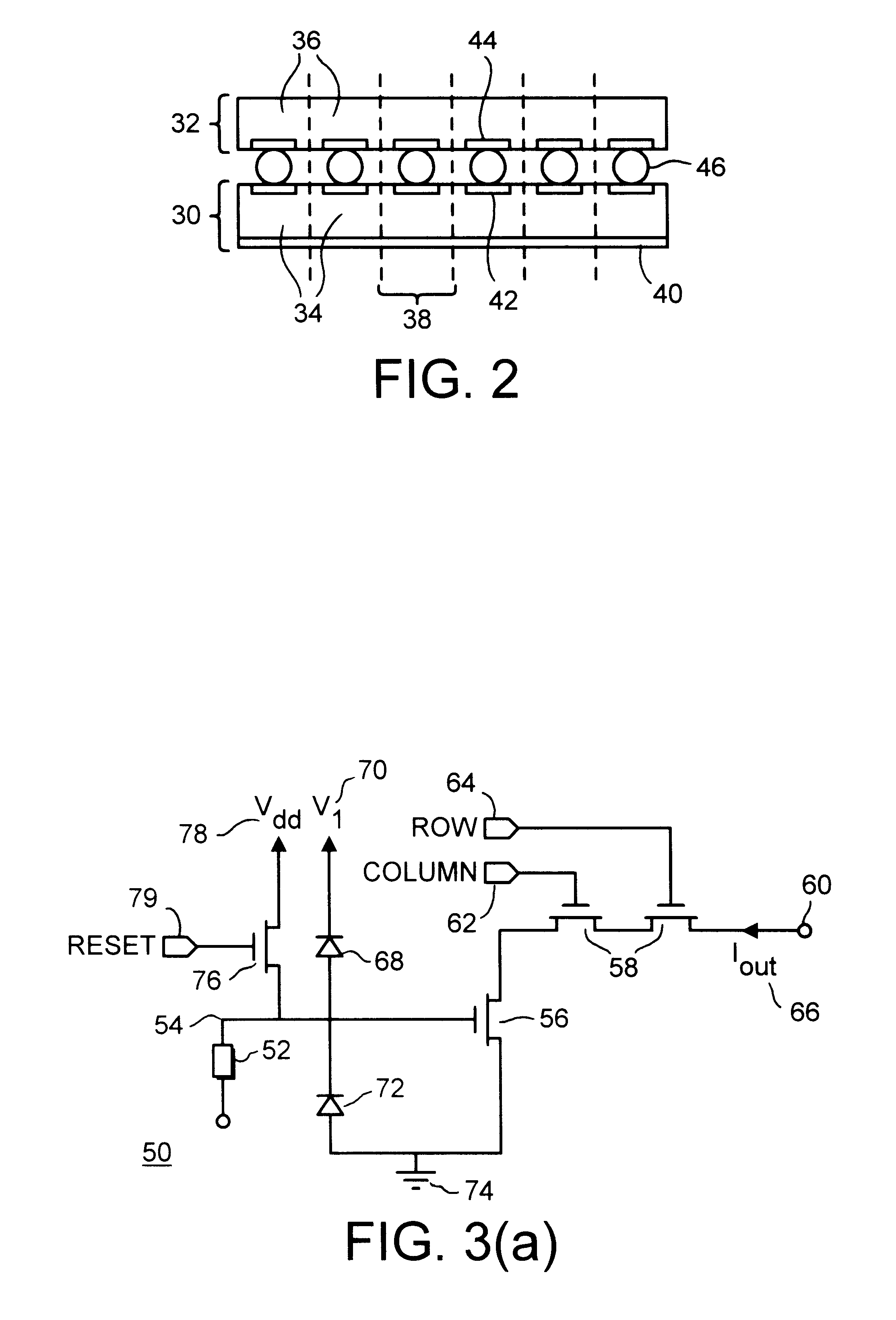
The imaging device 16 in FIG. 1 can consist of one or two semiconductor substrates. In case of one substrate, each cell 18 in the substrate comprises of a pixel detector...


PUM


Abstract

An imaging device for radiation imaging is an array of image cells. The array of image cells consists of an array of detector cells and an array of image cell circuits. Each detector cell is connected to the corresponding cell in the array of image cell circuits. Each individual cell in the detector cell array generates a charge based on the radiation that hits the cell. Each cell in the array of image cell circuits accumulates the charge on a storage capacitor. The storage capacitor can be, for example, the gate of a transistor. Single cells in the array of image cells can be grouped together to form larger area super cells. The size of the super cell can be controlled by control signals, which select the operating mode. The output from a cell, a single cell or a super cell, is read out in current mode and is scaled according to the size of the cell. The read out line is pre-charged prior to read out to reduce the effect of parasitic capacitance in the read out line. Several modes can be implemented in the imaging device. Also, an imaging system for larger area radiation imaging can be implemented by connecting several imaging devices together in form of a two-dimensional array.

Description

This invention relates to radiation imaging using a semiconductor imaging device consisting of an array of image cells.BACKGROUND TO INVENTIONThis invention describes a semiconductor imaging device for radiation imaging. The imaging device is an array of image cells, which consists of an array of radiation detector cells and an array of image cell circuits. An example of an imaging system configuration is shown in FIG. 1 of the accompanying drawings. All cells in the detector cell array are connected to respective electronics cells in the array of image cell circuits. With appropriate processing technology, it is possible to implement both detector cells and circuit cells on the same substrate. Another possibility is to have two substrates, one for the detector and one for the cell circuits and, by using a bump-bonding or other technique connect them mechanically and electrically together so that each detector cell is connected to the corresponding cell circuit. A cross-section of a...

Claims


Application Information

Patent Timeline
IPC IPC(8): H04N5/335H04N3/15H04N5/32
CPCH04N3/1562H04N3/1568H04N5/335H04N5/32H04N25/443H04N25/745H04N25/76H04N25/00
Inventor PYYHTIA, JOUNI ILARIERALUOTO, MARKKU TAPIO
Owner SIEMENS AG
Why Eureka
Try Eureka